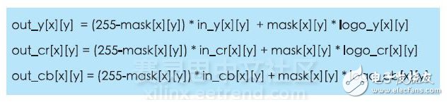
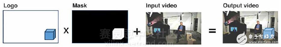
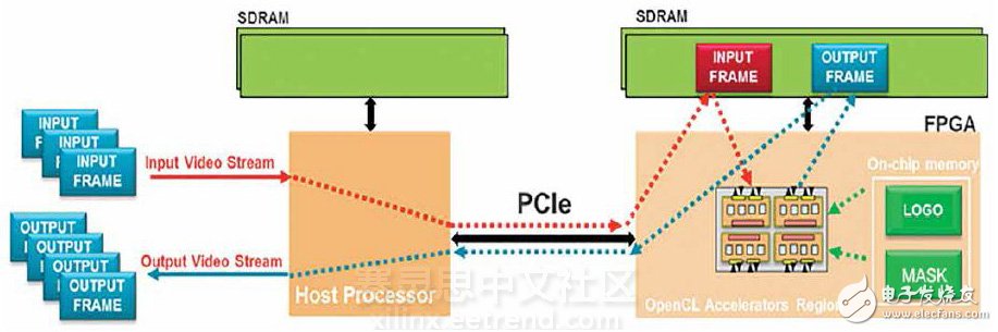
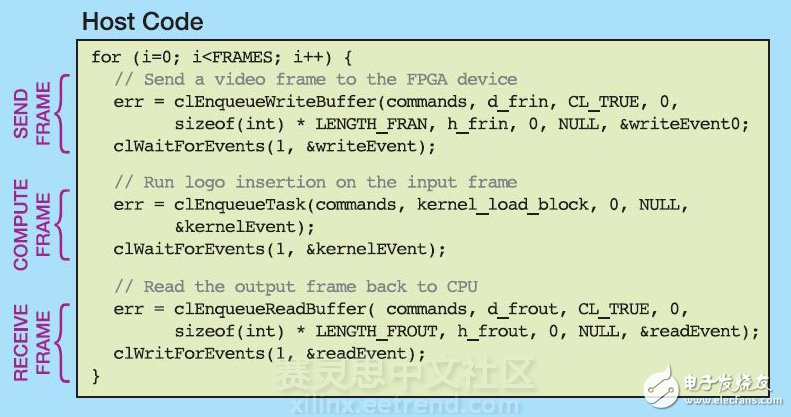
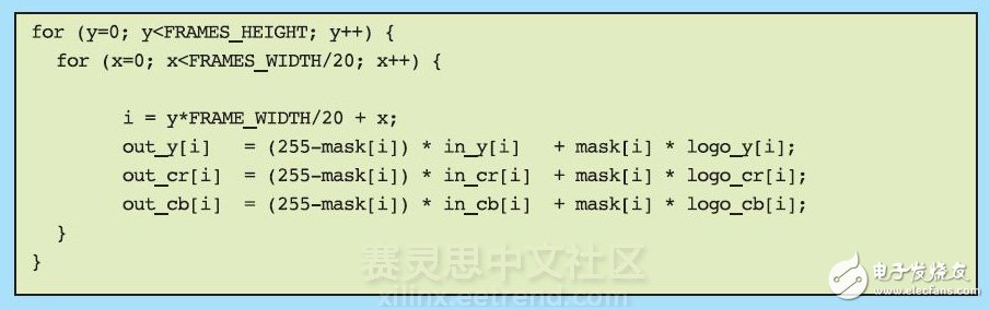
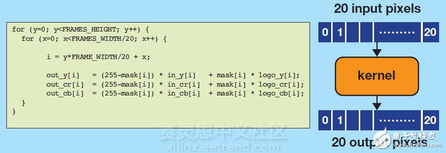
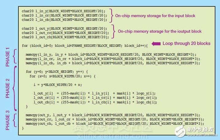
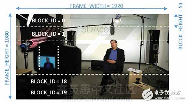
Xilinx SDAccel development environment provides optimization methods for memory limit issues Video streaming and downloads typically consume most of the Internet traffic of consumers, and are also a major driver of cloud computing technology. The growing demand for video streaming and downloading is driving video processing applications into the professional system arena and stepping into the data center. This shift in application model requires fast-expanding compute nodes to meet the varying high-intensity stages of video content production and distribution, such as transcoding requirements and watermarking requirements. We recently used the Xilinx SDAccel development environment to compile and optimize video watermarking applications written in OpenCL for FPGA accelerator cards. Video content providers use watermarks to serve as advertising and content protection. Our goal was to design a watermarking application that can handle high-definition (HD) video with a 30fps resolution and 1080p resolution running on an Alpha Data ADM-PCIE-7V3 card. The SDAccel development environment allows designers to write applications in OpenCL and then compile the application into the FPGA without having to understand the underlying FPGA implementation tools. This video watermarking application can be used as an example to introduce the main optimization techniques in SDAccel. Video Watermark with Identification Insertion Function The main function of this video watermarking algorithm is to cover an identifier at a specific location of the video stream. The identifier used for the watermark can be active or stationary. The activity logo is typically implemented using a short repetitive video clip, while the still logo uses a still image. The most common way for broadcasters to promote their own video streams is to use the corporate identity as a static watermark, thus becoming the target of our example design. The application inserts a stationary marker at a pixel-by-pixel granularity according to the following equation. The input and output frames are in a two-dimensional array, and the pixels are expressed using the YCbCr color gamut. In this color gamut, each pixel is expressed in three components. Y represents the luminance component, Cb represents the chrominance blue color difference component, and Cr represents the chrominance red color difference component. Each component is represented by an 8-bit value because each pixel is 24 bits. The logo is a two-dimensional image containing the content to be inserted. The mask is also an image, but only contains the outline of the logo. The pixels of the mask can be white or black. The white pixels of the mask indicate the insertion position of the logo, and the black pixels indicate where the original pixels are not touched. Figure 1 shows an example of the operation of this video watermarking algorithm. Figure 1 - Working Video Watermarking Algorithm Target System and Initial Implementation The system in which we run the application is shown in Figure 2. The system consists of an Alpha Data ADMPCIE-7V3 card that communicates with the x86 processor over a PCIe® link. In this system, the host processor extracts the input video stream from disk and transfers it to the device's global memory. The device's global memory is located on the FPGA card and is directly accessible to the FPGA. In addition to storing video frames in the device's global memory, the identification and mask are also transferred from the host to the FPGA accelerator card and stored in on-chip memory to take advantage of the low latency of BRAM memory. Because this application uses a static logo, you only need to store still images and layout location data in on-chip memory. Figure 2 - Overview of the Video Watermark Application System After the data is created, the host processor sends a start signal to the watermark core in the FPGA fabric. This signal triggers the kernel to complete three tasks: start fetching the input video frame from the device's global memory; insert the tag at the location defined by the mask; and transfer the processed frame back to the device global processor, waiting for the processor to call. The coordination of data transfer and calculation for each frame in the video stream is done using the code shown in Figure 3. Figure 3 - Code for Coordinating Data Transfer and Calculation Per Frame The code runs on the host processor and is responsible for sending video frames to the FPGA accelerator card, starting the accelerator, and then retrieving the processed frames from the FPGA accelerator card. The first implementation of the FPGA watermarking algorithm is shown in Figure 4. This is a functionally correct application implementation, but does not perform any performance optimization or to take into account the capabilities of the FPGA fabric. So after the code is compiled in SDAccel, the maximum throughput achieved on the Alpha Data card is only 0.5fps. Figure 4 - Initial implementation of the watermark kernel As can be seen from the code in Figure 4, this watermarking algorithm is not a highly computationally intensive design. Most of the time is spent accessing memory, reading and writing on video frames. So when we optimize the example design, we focus on optimizing the memory bandwidth. Optimizing Memory Access Using Vectorization One of the advantages of FPGA architectures is the flexibility to configure a bus that connects to memory compared to other software programmable architectures. SDAccel creates custom data paths and architectures for connecting memory based on the specific application kernel. By modifying the code, multiple pixels can be processed at a time, enabling higher memory bandwidth to be called from the kernel. This process is called vectorization. The appropriate degree of vectorization depends on the specific application and the FPGA accelerator card used. Taking the Alpha Data card as an example, the device's global memory interface width is 512 bits, which is consistent with the maximum AXI interconnect width that SDAccel provides for the kernel. Since the maximum bandwidth is 512 bits, the app adjusts to 20 pixels per processing (24 bits/pixel & TImes; 20 pixels = 504 bits). SDAccel fully supports vector data types. So for this application, the vectorization of the code is very simple, that is, the data type of all arrays is modified to char20 (as shown in Figure 5), so that the throughput can reach 12fps. Figure 5 - Vectorized kernel code Optimizing Memory Access with Burst Mode Although vectorization can significantly improve application performance, it is still not enough to achieve a throughput target of 30fps. The app is still limited by memory because the kernel can only transfer 20 pixels to memory at a time. To alleviate the impact of memory limitations on the application, we had to modify the kernel code to generate burst read/write operations into memory to achieve a data set larger than 20 pixels. The modified kernel code is shown in Figure 6. Figure 6 - Kernel code optimized for burst data transfer The first thing the code kernel modifies is to define on-chip storage in the kernel to store blocks of pixels each time. On-chip memory is defined by the array declared in the kernel code. To initiate a burst transaction to memory, the code instantiates the memcpy command to move the data block from DDR to the BRAM storage system within the kernel. According to the size of the on-chip memory resources and the amount of data to be processed, a video frame can be divided into 20 1920 & TImes; 54 pixel blocks (as shown in Figure 7). Figure 7 - Partitioning a video frame into data blocks When the memcry command places a block of data into the kernel array, the algorithm executes the watermark algorithm on the block and then puts the result back into the kernel array. The result of the block processing is then transferred back to the DDR memory using the memcry command. This operation is repeated 20 times until all the data blocks in the given frame have been processed. By modifying the kernel code, the system performance reached 38fps, exceeding the established 30fps target. Application prospects The necessary optimizations that are made when using SDAccel to develop such applications described in this article are software optimizations. So these optimizations are similar to the optimizations that get performance from other processing architectures such as GPUs. With SDAccel, the details of PCIe link work, drivers, IP layout, and interconnect are not a problem, making us just like designers to focus on developing target applications. The optimizations we made in the watermarking application apply to all applications compiled with SDAccel. In fact, the video watermarking application is a great example of a good example of the optimization method introduced in Xilinx SDAccel.
Galvanized monopole tower
1. Based on its shapes, it is generally divided into 5 types: Goblet type, cathead type, cathead type, shaped type and barrel type.
2. Their structural features are: All kinds of towers are of space truss structures; Bard are mainly composed of single equal angle steel or assembling angle steel; Materials are generally Q235(A3F) and Q345(16Mn); Bars are connected by black bolts with shearing force; Entire tower is composed of angle steels, link plates and bolts; A few components like tower base are assemblies of welded steel plates for convenience of hot galvanizing anti-corrosion, transportation and erection.
3. For steel towers that with height below 60m, shackles are mounted on one of main columns for construction people to climb to work. Our Company is a large scale enterprise specializing in manufacturing of 220KV (330KV) electric power steel tower with advanced manufacturing facility and international top-ranking assembly line.
Monopole Tower,Telecommunications Monopole,Steel Monopole Tower, Monopole Transmission Tower,Galvanized Monopole YIXING FUTAO METAL STRUCTURAL UNIT CO.,LTD( YIXING HONGSHENGYUAN ELECTRIC POWER FACILITIES CO.,LTD.) , https://www.chinasteelpole.com
Galvanized monopole Towers are used for a variety of communication applications and are ideal for use when zoning is difficult. Monopoles can also be designed as camouflage poles: pine tree poles, flag poles, palm poles and other stealth towers. Many uses include cellular monopoles, wireless internet monopoles, wifi tower, homeland security monopoles, two-way monopoles, and wind tower monopoles.
Based on application, it can be divided into: Strain tower, straight line tower, angle tower, transposition tower (tower for transposition of wire phase position), terminal tower and crossing tower, etc.