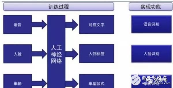
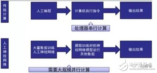
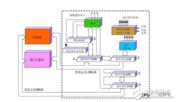
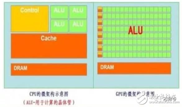
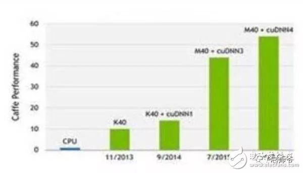
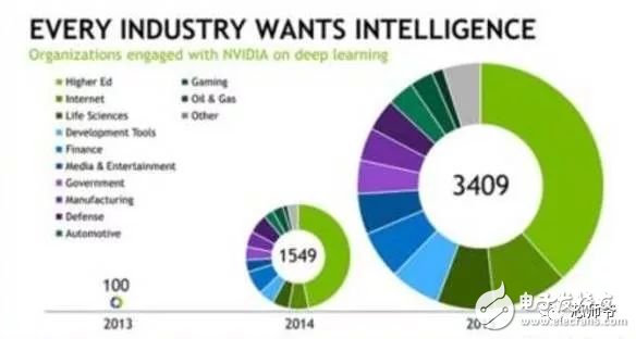
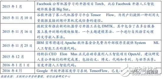
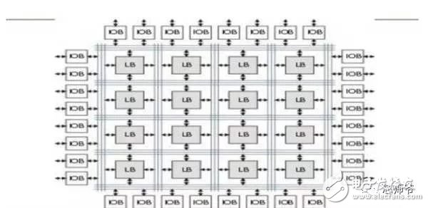
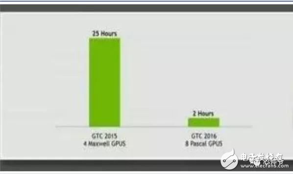
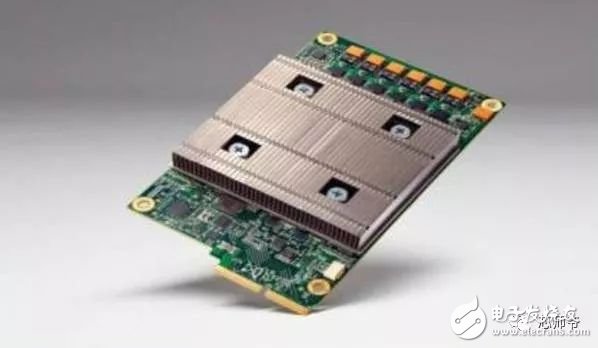
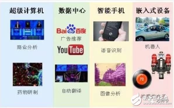
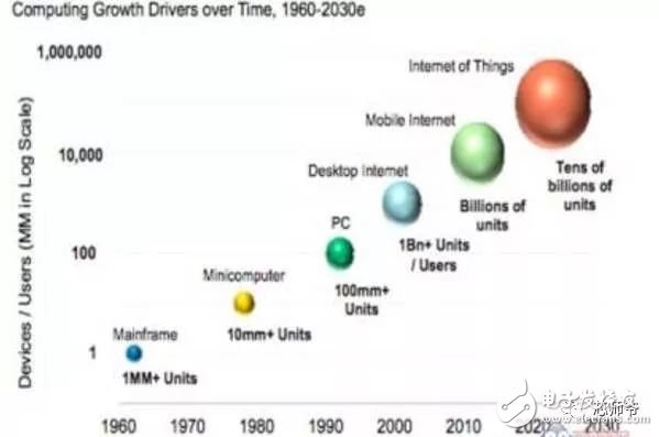
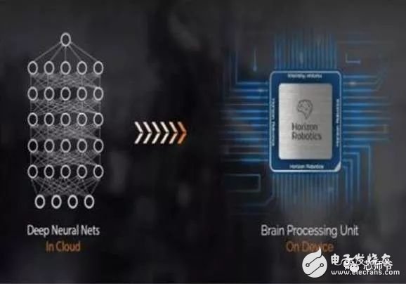
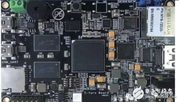
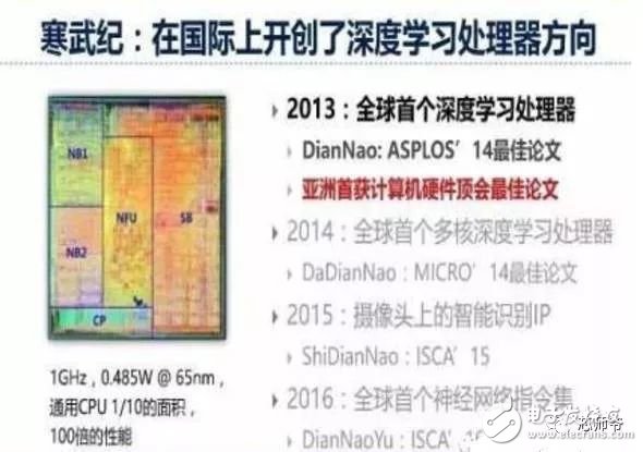
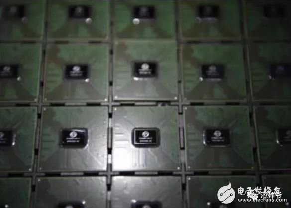
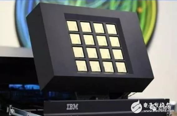
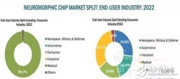
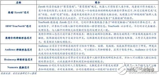
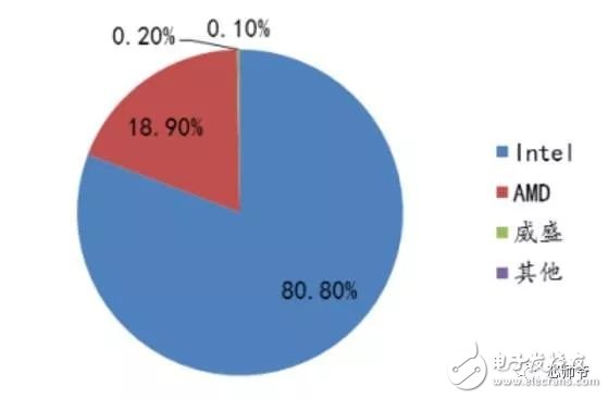
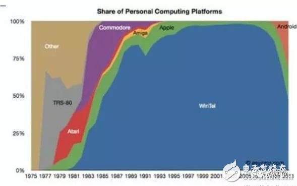
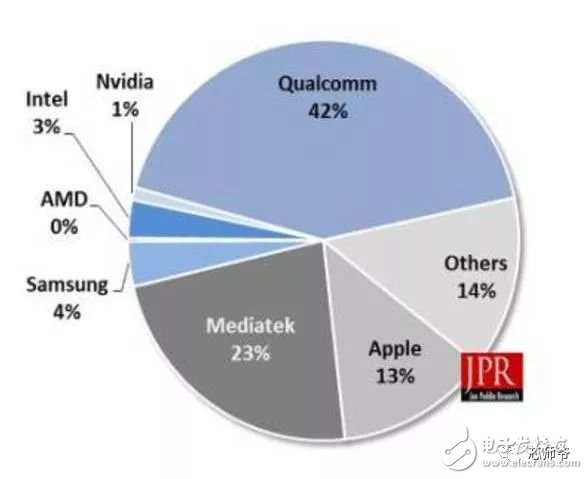
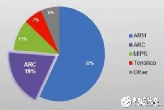
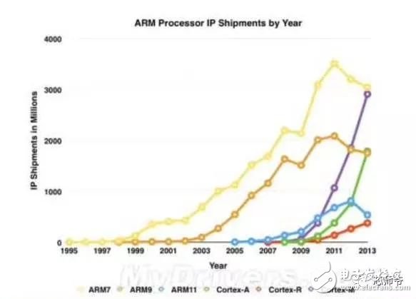
In the global technology field, artificial intelligence is undoubtedly the hottest area. This not-so-new application scenario will drive a new round of computing revolution, which will bring new demands to artificial intelligence chips and bring new opportunities to the semiconductor field. The purpose of artificial intelligence chip design is to accelerate the deep learning algorithm and hope to simulate the human brain from the underlying structure to achieve better intelligence. At present, artificial intelligence chips cover three stages: (1) FPGA-based semi-customization. (2) Full customization for deep learning algorithms. (3) Brain computing chip. Let's take a look at the research and development strategy of artificial intelligence chips from Essence Securities. Deep learning as a new generation of computing models, in recent years, its unprecedented breakthrough has set off a new wave of artificial intelligence development. Deep learning is essentially a multi-level artificial neural network algorithm, which is a neural network that mimics the human brain, simulating the operating mechanism of the human brain from the most basic unit. Because the operating mechanism of the human brain is distinct from that of computers, deep learning is very different from traditional computing models. The difference between the brain's operating mechanism and the current computer The artificial neural network algorithm of deep learning is different from the traditional computing mode. It can spontaneously sum up the regularity from the input of a large amount of data, and thus infers to the case that has never been seen before. Therefore, it does not require artificial extraction of the features required to solve the problem or summarize the rules for programming. The artificial neural network algorithm actually establishes the mapping relationship between input data and output data through a large amount of sample data training. The most direct application is in classification identification. For example, the input of the training sample is voice data, and the function of the trained neural network is voice recognition. If the training sample input is face image data, the function realized after training is face recognition. Deep learning is actually establishing a mapping between input and output data. The traditional computer software is programmed by the programmer according to the functional principle that needs to be realized, and can be input to the computer to run, and the calculation process is mainly embodied in the process of executing the instruction. The deep learning artificial neural network algorithm contains two calculation processes: 1. Train the artificial neural network with the existing sample data; 2. Use a trained artificial neural network to run other data. This difference increases the need for training data volume and parallel computing power, reducing the need for manual understanding of functional principles. Artificial neural network algorithm is different from traditional computing mode According to the above analysis, we can see that the biggest difference between deep learning and traditional computing mode is that no programming is required, but massive data parallel computing is required. Traditional processor architectures (including x86 and ARM, etc.) often require hundreds or even thousands of instructions to complete a neuron's processing and therefore cannot support the massively parallel computing needs of deep learning. Why can't traditional computing architectures support the massively parallel computing needs of deep learning? Because traditional computing architectures have limited computing resources. The traditional computing architecture is generally composed of a central operator (execution instruction calculation), a central controller (order execution of instructions), memory (storage instructions), input (input programming instructions), and output (output results). The integration of the operator and the central controller on a single chip constitutes the CPU we usually talk about today. CPU internal structure diagram (ALU only is the main calculation module) We can see from the internal structure of the CPU: essentially only a single ALU module (logical unit) is used to complete the calculation of the instruction data, and the other modules exist to ensure that the instructions can be executed one after another. This versatile structure is ideal for traditional programming calculation modes, and can increase the speed of the CPU by increasing the CPU frequency (to increase the instruction speed per unit time). But for a computational requirement that does not require too many program instructions, but requires the deep learning of massive data operations, this structure is very clumsy. Especially in the current power limitation, it is impossible to speed up the instruction execution speed by increasing the CPU frequency. This contradiction is increasingly irreconcilable. Therefore, deep learning requires new underlying hardware that is more adaptive to such algorithms to speed up the computational process, that is, new hardware plays a very important role in speeding up deep learning. The main way is to use the existing GPU, FPGA and other general-purpose chips. As a chip that meets the needs of image processing, the GPU's ability to parallelize massive data is in line with the requirements of deep learning. Therefore, it is the first to introduce deep learning. The arithmetic unit accounts for a small percentage of the CPU, and most of the GPUs are arithmetic units. In 2011, Wu Enda took the lead in applying it to Google's brain and achieved amazing results. The results showed that 12 NVIDIAD GPUs can provide deep learning performance equivalent to 2000 CPUs, followed by researchers at New York University, the University of Toronto, and the Swiss Artificial Intelligence Laboratory. Accelerate their deep neural networks on the GPU. NVIDIA GPUs increase the speed of training deep neural networks by 50 times Nvidia is the world leader in programmable graphics processing technology, and its core product is the GPU processor. NVIDIA quickly cuts into the field of artificial intelligence through the outstanding performance of GPU in deep learning, and greatly enhances its programming efficiency, openness and richness by creating NVIDIA CUDA platform, including CNN, DNN, deep sensing network, RNN, LSTM and A platform for enhancing algorithms such as learning networks. NVIDIA quickly established a general-purpose GPU acceleration platform that supports research institutions, industry giants and start-ups According to Nvidia’s public announcement, in just two years, NVIDIA’s companies in deep learning have surged nearly 35 times to more than 3,400 companies in medical, life sciences, energy, financial services, automotive, manufacturing. Industry and entertainment industries and other fields. Companies that have collaborated with NVIDIA on deep learning have proliferated nearly 35 times in two years NVIDIA develops GPUs for all types of intelligent computing devices, enabling deep learning to penetrate various types of smart machines On the one hand, the deep learning system needs to use huge data to train it. On the other hand, there are tens of thousands of parameters in the system that need to be adjusted. The IT giant's open source artificial intelligence platform is designed to mobilize more outstanding engineers to participate in the development of its artificial intelligence system. An open development platform will bring booming downstream applications. The most typical example is the Google open source Android platform, which directly contributes to the unprecedented prosperity of downstream mobile Internet applications. Take Google as an example. Users use the open source TensorFlow platform to train and export the artificial intelligence models they need, and then directly import the models into TensorFlow Serving to provide predictive cloud services. The TensorFlow series provides the entire deep learning model. The service plan is all inclusive. In essence, users of open source deep learning tools are directly transformed into their cloud computing services. Cloud computing service providers, including Ali and Amazon, embed machine learning platforms as a way to enhance their competitiveness and attract more users. Since 2015, the world's top AI giants have been vying for open source's core artificial intelligence platform, and various open source deep learning frameworks have emerged, including: Caffe, CNTK, MXNet, Neon, TensorFlow, Theano and Torch. Majors compete for open source artificial intelligence platform Looking back at the history of the computer industry, new computing models often spawn new specialized computing chips. The strong demand for new computing in the era of artificial intelligence is spawning new specialized computing chips. At present, the new computing requirements of artificial intelligence represented by deep learning mainly use GPU, FPGA and other general-purpose chips suitable for parallel computing to achieve acceleration. When industrial applications are not on the rise, the use of such existing general-purpose chips can avoid the high investment and high risk of specializing in the development of custom-made chips (ASICs). However, since such general-purpose chips are not designed specifically for deep learning, Naturally, there are bottlenecks in performance and power consumption. With the expansion of the scale of artificial intelligence applications, such problems will become increasingly prominent: The GPU is an image processor designed to cope with the need for massively parallel computing in image processing. Therefore, when applied to deep learning algorithms, there are three limitations: First, the advantages of parallel computing cannot be fully utilized in the application process. Deep learning involves two calculations: training and application. The GPU is very efficient in training deep learning algorithms, but it can only process one input image at a time. The advantage of parallelism cannot be fully realized. Second, the hardware structure is fixed without programmability. The deep learning algorithm is not completely stable. If the deep learning algorithm changes greatly, the GPU cannot flexibly configure the hardware structure like the FPGA. Third, running deep learning algorithms is much less efficient than FPGAs. Academia and industry research has proven that the same performance can be achieved by running deep learning algorithms. The power consumption of GPUs is much larger than that of FPGAs. For example, the artificial intelligence chips of domestic startups, Shenjian Technology, based on FPGA platforms, are relatively GPU-efficient in the same development cycle. There is an order of magnitude improvement. In addition, you need to talk about FPGA, the field editable gate array, which is a new type of programmable logic device. The original intention of the design is to realize the function of the semi-custom chip, that is, the hardware structure can be flexibly changed according to the needs of real-time configuration. According to the Xilinx report, the current FPGA market is dominated by Xilinx and Altera, which together share 85% of the market, with Altera being acquired by Intel for $16.7 billion in 2015 (this transaction is the largest amount ever involved in Intel's history) In the acquisition case, another Xilinx chose to work intensively with IBM, and behind it, the importance of FPGA in the era of artificial intelligence. FPGAs apply to deep learning research milestones Although the FPGA is highly optimistic, even the new generation of Baidu brain is based on the FPGA platform, but it is not developed specifically for the application of deep learning algorithms, there are still many limitations: First, the basic unit has limited computing power. In order to achieve reconfigurable features, there are a large number of very fine-grained basic units inside the FPGA, but the computational power of each unit (mainly relying on the LUT lookup table) is much lower than the ALU modules in the CPU and GPU. Internal structure of the FPGA Second, there is still a big gap between speed and power consumption compared to dedicated custom chips (ASICs); Third, FPGAs are more expensive. In the case of scale-up, the cost of a single FPGA is much higher than that of a dedicated custom chip. From the perspective of development trends, artificial intelligence custom chips will be the general direction of computing chip development: First, the performance improvement of custom chips is very obvious. For example, NVIDIA's first chip designed for deep learning from scratch, the Tesla P100, is 12 times faster than its GPU series in 2014. Google's custom-made chip TPU for machine learning boosts hardware performance to a level equivalent to 7 years after Moore's Law. NVIDIA designs chips for deep learning Tesla P100 12 times faster than GPUs released a year ago It should be pointed out that the rapid increase in performance is of great significance for the development of artificial intelligence. Dr. Chen Yunqi, a researcher at the Institute of Computing Technology of the Chinese Academy of Sciences and the founder of the Cambrian Deep Learning Processor Chip, wrote in the "China Computer Society Newsletter" that by designing a specialized instruction set, microstructure, artificial neural circuits, and storage hierarchy, it is possible In 3-5 years, the intelligent processing efficiency of the brain-like computer of the deep learning model is increased by 10,000 times (relative to the Google brain). The significance of 10,000 times improvement is that you can put a deep learning supercomputer such as Google Brain into your mobile phone to help us understand and recognize various images, voices and texts locally and in real time. More importantly, it has the ability to train in real time. After that, we can continuously improve our ability by observing people's behavior and become an intelligent assistant in our lives. Google TPU is equivalent to achieving hardware performance that has been developed for 7 years in accordance with Moore's Law. Second, the downstream demand is sufficient to dilute the cost of custom chip inputs. The market space of artificial intelligence will not only be limited to traditional computing platforms such as computers and mobile phones. From unmanned cars and drones to smart home appliances, devices that are at least dozens of times larger than smartphones need to introduce awareness. Interaction ability. Due to the requirements of real-time and training data privacy, these capabilities cannot be completely dependent on the cloud, and must have local hardware and software infrastructure support. From this perspective alone, the demand for artificial intelligence custom chips will be tens of times that of smartphones. Artificial intelligence core chip is widely used downstream Artificial intelligence will spawn dozens of core chip requirements for smartphones Third, companies that cut into artificial intelligence through algorithms hope to make profits through chip and productization. There are many companies that are currently cutting into artificial intelligence through algorithms, including companies that use algorithms such as speech recognition, image recognition, and ADAS (Advanced Driver Assistance Systems). Because they provide high-frequency, basic functional services, the commercial profitability of algorithms alone often encounters bottlenecks. Mobileye Releases Fourth Generation ADAS Vision Processor By chipping and productizing the respective artificial intelligence core algorithms, it not only improves the original performance, but also hopes to pave the way for commercial profit. At present, famous artificial intelligence companies including Mobileye, Shangtang Technology, and Horizon Robot are working on the core algorithm chip. Horizon robots are building deep learning localization chips At present, the tide of custom-made chips for artificial intelligence has gradually begun to emerge. Nvidia announced this year that R&D invested more than 2 billion US dollars for deep learning dedicated chips, and Google has even secretly run a TPU chip for deep learning for one year. The chip is directly Supported the world-wide Go wars that shocked the world. China's Cambrian chips are also scheduled to begin industrialization this year. Google's "AlphaGo" in the Habitat Game uses about 170 graphics processing units (GPUs) and 1200 central processing units (CPUs) that require a single computer room and high-powered air conditioning. As well as several experts for system maintenance. The number of chips currently used by AlphaGo will be replaced by a chip of the "Cambrian" architecture developed by the Chinese in the future. It is estimated that a small box will be fully loaded. This means that the "Alpha Dog" will be able to run faster. The emergence of artificial intelligence-specific chips indicates that the new round of computing model changes starting from the chip level has kicked off, which is the turning point for the artificial intelligence industry to formally mature. The purpose of designing the chip is to accelerate the deep learning algorithm and hope to simulate the human brain from the underlying structure to achieve better intelligence. At present, artificial intelligence chips cover three stages of FPGA-based semi-customization, full-customization for deep learning algorithms, and brain-like computing chips. Artificial intelligence chip development stage (1) Semi-customized artificial intelligence chip based on FPGA In the case that the chip demand has not yet become large, and the deep learning algorithm is not stable, it needs to be iteratively improved. It is the best choice to realize the semi-custom artificial intelligence chip by using the FPGA chip with reconfigurable characteristics. The outstanding representative of this type of chip is the domestic startup Shenkang Technology, which designed the "Deep Processing Unit" (DPU) chip, hoping to achieve better performance than GPU with ASIC-level power consumption. Its first products are based on the FPGA platform. Although this semi-custom chip relies on the FPGA platform, it can be quickly developed and quickly iterated by abstracting the instruction set and compiler. Compared with the dedicated FPGA accelerator product, it also has obvious advantages. Shenjian Technology FPGA Platform DPU Product Development Board (2) Fully customized artificial intelligence chip for deep learning algorithm These chips are fully customizable using ASIC design methods, and performance, power, and area metrics are optimized for deep learning algorithms. Google's TPU chip, the Cambrian deep learning processor chip of the Institute of Computing Technology of China's Chinese Academy of Sciences is a typical representative of such chips. The Cambrian has created a deep learning processor direction internationally Taking the Cambrian processor as an example, the current Cambrian series already contains three prototype processor structures: Cambrian No. 1 (English name DianNao, prototype processor architecture for neural networks), Cambrian 2 (English) Named DaDianNao, for large-scale neural networks), Cambrian No. 3 (English name PuDianNao, for multiple depth learning algorithms). Cambrian chips are planned to be industrialized this year Among them, Cambrian 2 has a frequency of 606MHz and an area of ​​67.7 mm2 in 28nm process, and the power consumption is about 16W. Its single-chip performance exceeds 21 times that of mainstream GPUs, while energy consumption is only 1/330 of that of mainstream GPUs. The 64-chip high-performance computing system can achieve up to 450 times better performance than mainstream GPUs, but the total energy consumption is only 1/150. (three) brain computing chip The design of such chips is no longer limited to just speeding up the deep learning algorithm, but at the basic structure of the chip and even at the device level, it is hoped that a new brain-like computer architecture can be developed, such as using new devices such as memristors and ReRAM. Increase storage density. The research on such chips has become a big gap from the mature technology that can be widely used on a large scale in the market, and even has great risks. However, in the long run, brain-like chips may bring about a revolution in the computing system. A typical example of such a chip is IBM's Truenorh chip. The TrueNorth processor consists of 5.4 billion connected transistors and consists of an array of 1 million digital neurons that can communicate with each other through 256 million electrical synapses. Truenorh chip integration neurons grow rapidly The chip uses a different structure than the traditional Von Neumann, fully integrating the memory, processor unit and communication components, so the processing of information is completely local, and because the amount of data processed locally is not large, the traditional computer The bottleneck between memory and CPU no longer exists. At the same time, neurons can communicate with each other conveniently and quickly. As long as they receive pulses (action potentials) from other neurons, these neurons will simultaneously act to implement event-driven asynchronous circuit characteristics. The chip consumes very little power because it doesn't require a synchronous clock: The 16 TrueNorth chips consume only 2.5 watts, which is comparable to a tablet. 16 Truenorh chips in a $1 million supercomputer at Lawrence Livermore National Laboratory The market for brain-like computing chips is huge. According to Markets-and-Markets, the market for brain-like computing chips containing consumer terminals will reach $100 billion by 2022, with consumer terminals being the largest market, accounting for 98.17% of the total, and other needs including industrial inspection, aviation, Military and national defense fields. 2022 brain-like computing chip market share forecast Brain-like chips of world-renowned chip companies The core chip will determine the infrastructure and future ecology of a new computing era. Therefore, global IT giants such as Google, Microsoft, IBM, and Facebook have invested heavily in accelerating the research and development of artificial intelligence core chips, aiming to seize the strategic high ground of the new computing era. Control the dominance of the artificial intelligence era. Looking back at the evolution of the X86 architecture and ARM architecture that dominated the PC and mobile Internet eras, we can see how important it is to gain a first-mover advantage from the source of the core chip architecture. The computer instruction set architecture can be divided into two types: complex instruction set (CISC) and reduced instruction set (RISC). The X86 architecture, which is monopolized in the PC era, is a complex instruction set. Complex instruction sets have inherent advantages in dealing with complex instructions, but at the same time there are problems of complex design, difficult flow, and high power consumption. PC processor market pattern (where Intel, AMD, and VIA are all X86 architectures) In essence, the streamlined instruction set was designed in the 1980s for the shortcomings of complex instruction sets. At the time, the academic community agreed that the streamlined instruction set was more advanced. However, the PC chip of the PC era, Intel's processor chip 8086, which was used before the invention of the reduced instruction set, adopted the X86 architecture of the complex instruction set. In the subsequent series of 80286, 80386 and other processor chips, the compatible X86 architecture continued to be adopted, while strengthening each A generation of processors is compatible with the upper layer software, and has established a Wintel alliance with Microsoft to firmly support the application ecology of the entire PC. The WINTEL Alliance monopolizes the computing platform of the PC market Software companies accustomed to using Intel X86 processors are no longer willing to use processors with other architectures, even if they perform better. The result: in the 1990s, almost only one Intel company insisted on developing X86-based processors, but defeated MIPS, PowerPC, IBM, HP, DEC, and other processors with reduced instruction sets. The X86 architecture was firmly in control. The dominance of the PC era. In the era of mobile Internet, Intel did not continue its advantages in the PC era, but a previously unknown British chip design company ARM became the new dominant of monopoly mobile processor chips. ARM licensed chip design IP business model There are three reasons for ARM's success: First, ARM started out as a CPU for Apple in the early 1990s (ARM was jointly funded by Acorn, Apple, and VLSI Technology), so it entered this fast-growing market at the beginning of the smartphone revolution. Apple's relationship laid the first advantage of its architecture in the mobile processor market; Second, the ARM processor is part of a reduced instruction architecture, and the X86 processor is inherently less power consuming than the complex instruction architecture, which is extremely important in the mobile market; Third, ARM created a business model that only authorized core design IP to not produce chips, and quickly wooed the major chip giants to establish their own ecological alliance. Mobile processor market share (Qualcomm, MediaTek, Apple, Samsung, etc. all adopt ARM-licensed architecture) The implications of ARM's success are: First, when the new era of computing comes, it is often an excellent opportunity for emerging companies to overtake the corners, and the strong traditional giants will inevitably face a reshuffle; ARM occupies more than half of the embedded processor IP, which accounts for more than 90% of mobile handset processors Second, grasp the first-mover advantage of the core chip architecture, and quickly establish an ecosystem based on this is the key to success in the era of a new computing change. Third, the currently used GPUs and FPGAs are not artificial intelligence custom chips, which have natural limitations. Artificial intelligence chips are the same blue line for giants and start-ups. ARM's various mobile processor sales, more than half of which were achieved after the rise of the mobile Internet era in 2009 We are in the midst of an important turning point from the information age to the intelligent era. Artificial intelligence will promote a new round of computing revolution, and the chip industry as the industry's most upstream is the pioneer of the artificial intelligence era: on the one hand, it has the meaning of industry leading indicators. On the other hand, it is also the industry that is the first to start and the most flexible in the early stage of the development of artificial intelligence industry. In the information age, there are billion-dollar chip giants like Intel. The era of artificial intelligence with a larger application market will surely breed more "Intel."
The military Wire Harness is an industry applied in the military, and the arms industry is a powerful industrial sector.
In China, the military industry mainly refers to the industrial departments and factories and other military units that mainly serve the national defense construction and directly provide weapons and equipment and other military supplies to the troops. Weapons products mainly include the weapons industry, aviation industry, shipbuilding industry, electronics industry, nuclear industry, aerospace industry, etc. The main products are guns, ammunition, tanks, military vehicles, military aircraft, military ships, military electronic equipment, rockets, missiles, military aerospace equipment, nuclear weapons and military clothing.
Typical requirements for military wire harnesses:
With our diverse capabilities and certifications, Kable-X is proud to be a top military Cable Assembly manufacturer. Kable-X's robust quality assurance process ensures that we meet all documentation requirements, product configuration and verification requirements. All finished cable assemblies have undergone strict continuity, resistance, mechanical integrity and withstand voltage electrical tests to ensure reliability and performance under any conditions.
Military Wire Harness,Military Cable Assembly,Wire Harness Specialist,Mil Spec Wire Harness Kable-X Technology (Suzhou) Co., Ltd , https://www.kable-x-tech.com


Excellent optical performance;
Strong connections to withstand shock and vibration;
Operating temperature range from -55°C to +125°C and beyond;
Lightweight design and compact size;
Combining high density and high channel count;
Low sensitivity to corrosion, pressure and humidity.
