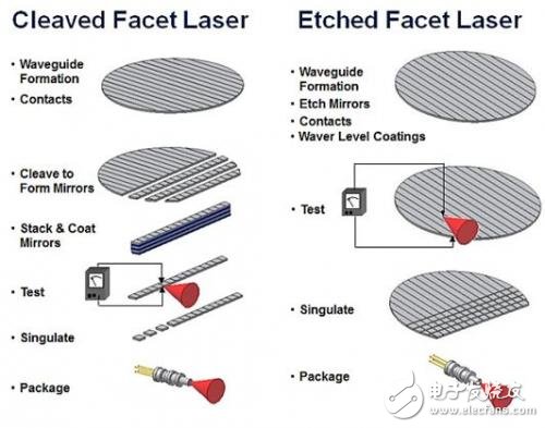
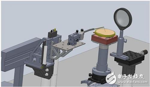
Computing and data communication organizations have always wanted to discover the latest in data speed and computing power. Many industry experts believe that chip-to-chip and on-chip photonics technology will be the most important technology affecting future computing. The silicon optoelectronic technology competition is in full swing, and hardware manufacturers are keen to share the $2 billion big cake. While the use of on-chip lasers has been around for many years, the high cost associated with manufacturing, testing, and calibration has hampered the widespread adoption of silicon photonics applications. Figure 1 shows how a semiconductor wafer based on indium phosphide (InP) is cut into strips to form a mirror for an edge emitting laser. These crystal strips are stacked one on another vertically and then a mirror coating is applied to the cleavage surface. A large number of crystal strips will form during the cleavage process, and each laser on each strip needs to be tested to determine its function. However, the test of the crystal bar requires the operation of these fragile semiconductor crystal strips by hand or machine, and generally one at a time. This process is therefore quite slow and expensive, and is limited to room temperature testing, so that the tester does not take too long to measure a strip. The fragile crystal strip must be handled with great care and gentleness during the test, otherwise the laser on the strip is easily damaged. Figure 1: The fabrication steps of the cleave plane and the etched surface laser indicate that they use different processes. After passing the test of the crystal strip, the crystal strip is continuously cut into individual laser chips and then calibrated with the silicon photonic chip in an active manner. This process is also expensive because the laser chip must be powered and moved during the calibration process until sufficient light is coupled into the silicon photonic waveguide. At this point, the position of the laser chip needs to be permanently locked to the silicon photonic chip. Since only the room temperature test was performed on the laser on the crystal strip, we still do not know if the laser has acceptable performance at the extreme temperature within the operating range. Because of this unknown condition, the Cleaved Facet Lasers silicon photonic chip must also be tested over the entire temperature range, which in turn requires additional resources and adds more cost. Hybrid silicon lasers, such as those developed and used by Intel for silicon photonics applications, use glass glue to fuse InP wafers and silicon wafers instead of the "flip-chip" approach of other laser technologies. The advantage of this method is that calibration is not required because the result of further processing after attaching InP to the silicon base is a silicon laser. The disadvantage is that there is no way to test the InP wafer before integration with the silicon substrate, so if the InP on a given silicon photonic chip is bad, the chip can only be discarded. As shown in Figure 1, the etched face technique (EFT) allows for the determination of crystal faces by high precision lithography rather than inaccurate, random mechanical cutting methods. Photolithography allows the position of the cavity and the position of the face to be within 0.1 μm. The result is unprecedented consistency and yield, and the ability to build structures that traditional technology cannot build. With the etched face technology, the device surface is formed with exceptional precision, enabling low-cost, passive calibration of silicon-based photons. The accuracy of active calibration can be achieved simply by the cost of an automated process. Figure 2: The lens captures light from the etched surface laser to be tested. The wafer probe performs a photo-current-voltage test on a laser that is still on the wafer. The photo-current-voltage (LIV) test is common to all laser types. The laser is first collected by a lens and then directed to the detector for light intensity measurement. For edge-emitting etched surface lasers, the general lens only collects a portion of the laser, so the actual optical power is also determined by calibration factors. Full spectrum testing can be performed at different currents and temperatures to ensure that the device has the desired performance over the entire operating temperature range. In this case, the laser from the lens is directed to the spectrum analyzer. Finally, for low temperature conditions, a transparent chamber is added to the test unit, and the chamber is filled with nitrogen to prevent condensation from forming on the wafer at low temperatures. There are many different ways to harness the enormous potential of silicon photonics applications, each with its own benefits and challenges, depending on the specific application. Ultimately, only by trying to overcome cost, yield and performance barriers can we succeed in this emerging industry. The ability to provide lasers with known qualified chips will be an important factor in the company's emergence. Lithium Battery Pack,6V Lithium Battery Pack,6 Volt Lithium Battery,Crv3 Lithium Battery Jiangmen Hongli Energy Co.ltd , https://www.honglienergy.com
This article will introduce and compare various laser technologies used in the field of silicon optoelectronics, including cleave planes, hybrid silicon lasers, and etched surface techniques. We will also delve into the testing methods used in various technologies to examine how testing can play an important role in driving cost reductions and promoting the widespread adoption of silicon photonics. 
One possibility is to do a full-temperature stripe-level test and produce a laser chip with a known qualified die (KGD), but this is not only expensive, but also very slow, because the laser bar has only a few devices. Moreover, during the test, the crystal strip needs to be placed at both extreme temperatures of cold and heat.
Since the InP wafer is fused to the silicon wafer, the actual InP area required for this method is generally large, substantially equal to the size of the silicon photonic chip. The cleave plane and the etched surface laser have advantages in this regard because only the laser cavity and its bond pads require expensive InP. However, if a developed process allows placement on a silicon photonic wafer from InP For wafer microchips, there will be a significant reduction in the number of InPs used.
Wafer-level laser testing can also be performed because the laser can be completely formed under the condition that the wafer is intact (and the wafer must be diced during the formation of the cleavage surface laser). Assuming thousands or tens of thousands of lasers on a 2-inch or 3-inch wafer, testing wafers to extreme temperatures during wafer-level testing will be extremely cost-effective, depending on the silicon photonic application requirements.
Another benefit is that the etched surface laser can be fully fabricated and automated tested before being split into individual chips. For example, using an in-house custom test equipment for etched face lasers, BinOpTIcs can provide InP-based lasers for qualified silicon photonic applications. All lasers on the wafer are tested with automated, high-throughput test operations over the entire temperature range required for silicon photonic applications.
Figure 2 shows the operation of an automated wafer-level test station for testing etched-surface lasers, showing a wafer table with an etched-surface laser on it. At the location away from the wafer table, there is a large lens for capturing the laser light from the etched surface laser during testing on the wafer. During the test, the wafer stage moves the wafer in the xy plane, leaving the position of the device under test and the lens unchanged. The probe arm carries the probe to the surface of the wafer and performs various tests on the laser. 