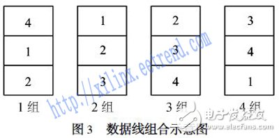
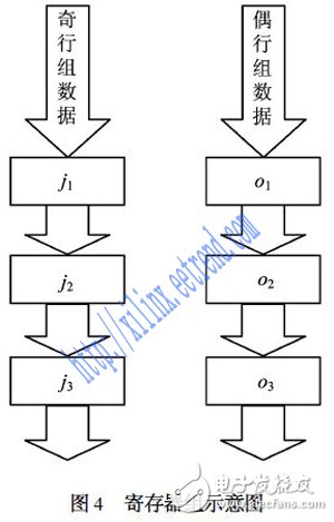
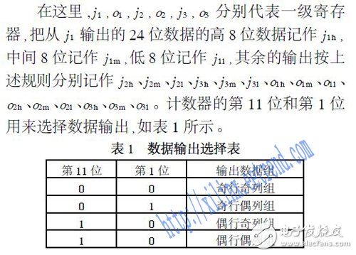
Abstract: An FPGA-based bilinear CFA interpolation algorithm is implemented. The algorithm is processed by XGA @15 Hz Bayer template data with 8 bits per pixel, in order to obtain XGA @15 Hz color image data of 24 bits per pixel. The input data first enters the cache module. The cache module is composed of dual-port RAM inside the FPGA. The data output from the cache is divided into odd row groups and even row groups, and then the data of the odd row group enters the odd row odd column operation block through the selector. And the odd row operation block, the data of the even row group enters the even row odd column operation block and the even row even column operation block by the selector, and finally, under the action of the interpolation control module, the data processed by each operation block is output by the output selector. . Digital image devices such as digital cameras, in view of cost and packaging, generally output a Bayer template [1] CFA (Color Filter Array) image, which requires a CFA interpolation algorithm to obtain a full-color image. When implementing an algorithm, a dedicated DSP (digital signal processing) is usually required, and then implemented in C language or other language programming; with the development of semiconductor technology, an FPGA (field pro-gramming gate array) is used as a programmable chip. The integration level has reached tens of millions of gates. The programmable features of FPGAs play an increasingly important role in SOC (system on a chip), which results in the implementation of algorithms directly with FPGAs without the need to reuse them. The expensive DSP, I tried to implement CFA interpolation algorithm based on FPGA. The bilinear interpolation algorithm [2,3] is a type of non-adaptive algorithm that uses a linear averaging calculation of the same color components in neighboring pixels to compensate for the missing color of each pixel. As shown in Figure 1, the pixels (2, 3) have only blue components. Therefore, the missing green portion can be obtained by averaging the green components of the upper, lower, left and right pixels. Similarly, the missing red can be averaged by the red component of the pixels on the adjacent four diagonals. This algorithm can be accepted by video because human eyes are not easily aware of blur in dynamic two-frame video. The entire design adopts a top-down modular design [4] method, the code is written in VHDL language, the top-level module is defined as CFA interpolation module, defines the input and output interface signals, reset, clock signal, and describes the internal sub-modules Logical connection relationship. The lower layer of the top layer is composed of 3 modules. The block diagram is shown in Figure 2. The design content is as follows: In the design of this module, considering the factors of real-time processing, when each frame of image comes in, two banks are written first, and the length of each bank is exactly equal to the number of effective pixels per line, and both are stored. The row is a valid pixel, and when the third valid pixel in the third row is written, the bank is read. The order in which the data is stored in the cache is such that the first row of the first frame of the image is stored in the No. 1 bank, and then stored in the first row, and the fifth row of data is stored in the No. 1 bank, so that the loop can be saved. After one frame is completed, the write controller is reset, and the next frame is followed by the above operation, so that it reciprocates. The cache controller writes to the cache by operating only one bank at a time, while the read operation is performed simultaneously on four banks. 2) Cache module. The module consists of four identical 1024 & TImes; 8 bit banks. Each bank is composed of two BLOCKRAMs inside the FPGA. Each bank is a dual-port SRAM, and one of the ports is defined as write-only. The other port is defined as read-only. Each port of each bank is operated by a read/write enable signal sent from the cache control module. The four banks are numbered, and are sequentially 1, 2, 3, and 4 banks. The banks 1 and 3 are referred to herein as odd rows, and the banks 2 and 4 are referred to herein as even rows. 3) Interpolation module. This module consists of 2 sub-modules, an interpolation control module and an interpolation operation module. The interpolation control module first combines the data lines input by the bank and numbers the combined data lines, as shown in FIG. 3, and the numbers in the boxes in FIG. 3 respectively represent the data lines output by the respective banks, and after such combination, , a 24-bit wide data line is obtained, and the high and low bits of the data line are also in the order shown in the figure. Taking one group as an example, the highest bit of the data line of the bank 4 is the highest bit after the combination, and the data of the bank 2 The lowest bit of the line is the lowest bit after the combination. Here, groups 1 and 3 are called odd rows, and groups 2 and 4 are called even rows. The interpolation control module has a 12-bit counter inside. The highest bit controls whether the data entering the interpolation module is 1, 2 or 3 or 4. The data of the parity group enters the respective 3-level register group, as shown in Figure 4.
Outdoor Fixed LED Display is a popular product for its high quality, every year sold to at least 80,000 pieces around the world, including Europe, North America, southeast Asia.Compared to other indoor LED display in the market, its biggest advantage is that it can display high-definition images while maintaining low power consumption.Besides, it adopts Die casting aluminum cabinet which is ultra-thin and ultra-light and owns good heat dissipation.Easy to install and maintain and suitable for multiple indoor scenes.
Application:
Movie theaters, clubs, stages.
Outdoor Fixed LED Display,Led Wall Display Screen,Curved Led Display Screen,Led Display Board Guangzhou Chengwen Photoelectric Technology co.,ltd , https://www.cwledpanel.com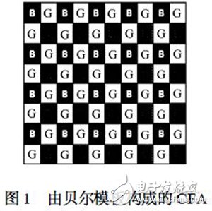
1) Cache control module. Two controllers are designed, one of which is the write controller and the other is the read controller. The write controller is mainly composed of a 12-bit counter. The upper two bits are used to select four banks, the lower ten bits are used to generate the corresponding address, and the buffer is written in accordance with the input write signal. The read controller consists primarily of a 10-bit counter that generates the address for the read operation of the four banks. 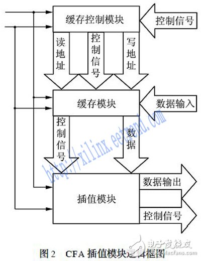
* Business Organizations:
Supermarket, large-scale shopping malls, star-rated hotels, travel agencies
* Financial Organizations:
Banks, insurance companies, post offices, hospital, schools
* Public Places:
Subway, airports, stations, parks, exhibition halls, stadiums, museums, commercial buildings, meeting rooms
* Entertainments: