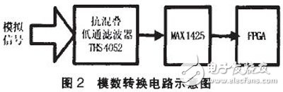
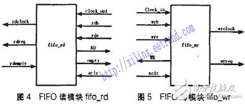
In recent years, FPGAs have been able to flourish in their applications, in the fields of communications, aerospace, medical equipment, and consumer electronics. The technology of using FPGA to control CF has not matured so far. This paper introduces the interface design between FPGA and CF card from the perspective of hardware and software, gives the programming of accessing CF card with dual RAM, and uses FPGA as FIFO to AD. The collected data is buffered and then stored in a large-capacity CF card. The data storage and acquisition system consists of three parts: CF card storage, FPGA data double buffer, status register and A/D converter. 2) FPGA mainly uses the internal SRAM to provide double buffering of data output/input. The reason for using double buffering is to prevent data overflow and ensure the continuity of data transmission. When the full message is received, the AD acquisition is stopped and a prompt is made. 3) The function of the A/D converter is to convert the analog quantity to be acquired into a digital quantity; after filtering and amplifying, it is received, buffered and stored by the FPGA to the CF card. The high speed AD converter uses the MAX1425 with a conversion rate of 20MHz. The working process of the system is as follows: the system sends a sampling start control command to the data acquisition system through the low level of an external button, and the FPGA sends a corresponding control signal to the AD converter according to the command; since the ADC sampling rate is 20 MHz, the storage speed is CF card. Matching, a FIFO buffer is generated inside the FPGA. The AD converter converts the analog signal into a digital signal under the control of the ADC interface control circuit of the FPGA, and stores the sampled data into the FPGA internal FIFO buffer. At the same time, the FPGA queries whether the CF card has capacity. If the CF card is not full, the CF card interface control logic of the FPGA sends the sampling result from the FPGA internal FIFO buffer to the CF card. When the capacity of the CF card reaches a certain level, the FPGA issues a full message, sends a command to stop the acquisition to the AD state machine, and prompts the user to be full. Since the FPGA is set to a specific automatic mode, the FPGA controls the AD acquisition and all operations between sending the data to the CF card without external intervention, thus ensuring sufficient data transfer rate. During the sampling process, the CF card interface control logic of the FPGA takes the batch data in turn. The AD continues to convert while the CF card is being stored, and the FPGA internal FIFO is continuously written to the conversion result. The hardware of the system consists of an analog-to-digital conversion interface circuit, a data storage and transmission control circuit, and an interface circuit. The analog-to-digital conversion interface circuit is an important part of the whole system. It consists of a low-pass filter, a multiplexer switch and an AD converter, as shown in Figure 2. The core device that plays this role in the system is the AD14, an AD conversion chip. The analog input signal is removed by an anti-aliasing low-pass filter consisting of the op amp THS4052, respectively, to prevent the signal from "aliasing." The analog-to-digital converter MAX4125 converts analog signals into digital signals. The control signal of the MAX4125 is provided by the FPGA board. The MAX4125 performs the conversion operation at the appropriate timing under the control signal. The development of data acquisition and transmission control circuits is mainly focused on FPGAs. The FPGA is responsible for buffering and controlling between the CF card and the ADC chip. One interface with the ADC and the other side with the CF card, generating all the control signals required for data acquisition, AD conversion, and FIFO. Enables buffering of transfer data, read/write control, clocking, output enable, and control of the ADC. 2_2.1 FPGA internal design From the data flow direction, the data is sent to the FIFO of the FPGA through the ADC interface under the coordination of the ADC interface control state machine. After buffering by the FIFO, the data is transmitted to the CF card outside the FPGA under the coordination of the CF card control state machine; When the CF card is full, the FPGA stops the acquisition of the AD through the ADC state machine and prompts the user to replace the CF card. The FIFO is mainly composed of three parts: FIFO body, FIFO read module, and FIFO write module. The FIFO body part uses the internal RAM of the FPGA to generate the used FIFO through the coregenerator. The FIFO read module and the FIFO write module mainly receive the read and write start and stop pulse signals given by the outside world, and convert them into read/write request signals, which are sent to the fifo body, and the read/write module processes the clock signals on both sides of the interface, respectively It is used as the read/write clock of fifo. The specific structure is shown in Figures 4 and 5. A good day usually starts when the sun rises, and bright light can improve our vision. The only exception is that due to excessive exposure to the sun, the screen will almost become insufficient due to reflections. Matte Hydrogel Screen Protector Sheet,Flexible Hydrogel Matte Screen Protector,Matte Hydrogel Screen Protector,Matte Anti-Glare Protective Film Shenzhen TUOLI Electronic Technology Co., Ltd. , https://www.szhydrogelprotector.com
1) CF card data storage, its role is to store the data collected by AD, when the data capacity is full, send full information. After the FPGA obtains full information, it stops collecting data and prompts the user to replace the CF card. 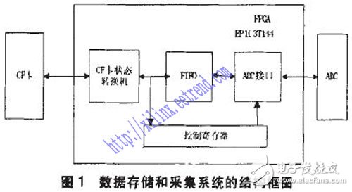
The internal structure of the FPGA design is shown in Figure 3. It consists of three parts: FIFO, CF card control state machine, and ADC interface control state machine. The wide arrow from right to left in the figure indicates the data stream, and Fd[15:0] is the data bus connected to the CF card. The single-line arrows indicate the input and output and the control signal lines between the various modules inside the FPGA. 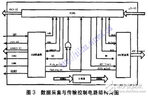
In order to solve the problem that you can enjoy the sun and read the phone screen at the same time, please install an Anti-glare Matte Screen Protector on the screen. Since the surface of the Screen Protective Film is matte, it has an anti-glare effect, and you can see the screen clearly without feeling dizzy.
The Frosted Screen Protector also allows you to sit on the beach during the holidays, or sunbathe on the balcony with your mobile phone or laptop at home, check emails, read or watch movies. Thanks to the Matt Screen Protector and its anti-glare function for laptops, smartphones, etc., electronic devices can be used even in bright sunlight.
In addition, the Matte Protective Film uses an oleophobic and waterproof coating to eliminate grease and dirt, thereby greatly reducing the formation of greasy fingerprints on the display. Please maintain a clear vision when exposed to the sun.