EDA is an acronym for Electronics Design Automation, which evolved from the concepts of Computer Aided Design (CAD), Computer Aided Manufacturing (CAM), Computer Aided Test (CAT), and Computer Aided Engineering (CAE) in the mid-1960s. of. EDA technology refers to the computer-based work platform, which combines the latest achievements of application electronics technology, computer technology, information processing and intelligent technology to automate the design of electronic products. The design file is completed with the hardware description language VerilogHDL, and then the logic is automatically compiled, simplified, segmented, integrated, optimized, laid, routed and simulated by the computer until the adaptation, logic mapping and programming download for the specific target chip. . The emergence of EDA technology has greatly improved the efficiency and operability of circuit design and reduced the labor intensity of designers. With EDA tools, electronic designers can design electronic systems from concepts, algorithms, protocols, etc. A lot of work can be done by computer, and the whole process of electronic products from circuit design and performance analysis to designing IC layout or PCB layout. The automatic processing on the computer is completed. (1) Front-end design (system modeling RTL level description) Back-end design (FPGAASIC) system modeling. (2) IP multiplexing. (3) Front-end design. (4) System Description: Establish a mathematical model of the system. (5) Function description: Describe the behavior of the system or the data flow diagram between each sub-module. (6) Logic design: Structure the system functions, usually with text, schematic, logic diagram, Boolean expression to represent the design results. (7) Simulation: including functional simulation and timing simulation, mainly verifying the correctness and timing characteristics of the system functions. (1) The code lock input circuit KEYB0ARD.VHD has unique features for the design of various frequency-divided signals/signal sequences. In this design, a free counter is used to generate various required frequencies, that is, an N-bit counter is first established, and the size of N is determined according to the requirements of the circuit. The larger the value of N, the more times the circuit can be divided, so that a larger frequency change can be obtained to provide a plurality of clock signals of different frequencies. If the input clock is CLK and the output of the N-bit counter is Q[N-1,0], then Q(0) is the divide-by-2 pulse signal of CLK, and Q(1) is the divide-by-4 pulse signal of CLK, Q( 2) is the div divided by 6 pulse signal, ... Q (N-1) is the 2N divided pulse signal of CLK; Q (5DOWNT04) is a pulse waveform sequence, the value is based on 00, 01, 10, 11, 00, 01 periodically change, the frequency of change is 5% of the CLK, which is 32 divided. We can use the above rules to get a variety of signals or signal sequences of the frequencies we need. (2) The design program of keyboard input debounce circuit DEBOUNCING.VHD has a good reference value in the development of actual system. (3) The password lock control circuit CTRL, VHD is better for updating and shifting data. In the program, the statement "ACC"=ACC(11DOWNT00)&DATA_N" is very succinctly realized that the lower 4 bits in the ACC are updated with DATA_N, and the upper 12 bits are processed by the original lower 12 bits in the ACC. . (4) In the design and simulation of the program of the module such as the password lock input circuit, in order to facilitate observation of some intermediate results, some observation output points are added to the program. This design technique is very important for the design of larger programs or multi-process programs. At the same time, in the simulation, in order to facilitate the observation of the global results, the frequency division constant is reduced. Similarly, when performing program simulation, it is necessary to modify the number of division/count/time constants in the program. EDA is an electronic design automation. The general university EDA class is about FPGAs, and some are slightly CPLD. The FPGA is a field programmable gate array. It is a programmable chip. You can program it into a microcontroller. It is a microcontroller. You can make it into other ones. Designing FPGAs requires EDA (Electronic Design Automation) aids, which are the tools for developing chip designs from chip developers, and compiling simulation software provided by third parties. EDA plays a huge role in teaching, research, product design and manufacturing. In terms of teaching, almost all universities of science and engineering (especially electronic information) have opened EDA courses. It is mainly to let students understand the basic concepts and basic principles of EDA, master the rules of writing in HDL language, master the theory and algorithm of logic synthesis, use EDA tools to conduct experimental verification of electronic circuit courses and design simple systems. General learning circuit simulation tools (such as multiSIM, PSPICE) and PLD development tools (such as Altera/Xilinx device structure and development system) will lay the foundation for future work. In scientific research, circuit simulation tools (multiSIM or PSPICE) are mainly used for circuit design and simulation; virtual instruments are used for product testing; CPLD/FPGA devices are actually applied to instruments and equipment; PCB Design and ASIC design are engaged. In product design and manufacturing, including computer simulation, EDA tool application in product development, system level simulation and simulation of test environment, EDA technology application of production line, product testing and other aspects. Such as PCB production, electronic equipment development and production, circuit board soldering, ASIC manufacturing process. From the application field, EDA technology has penetrated into all walks of life, as mentioned above, including EDA applications in various fields such as machinery, electronics, communications, aerospace, chemical, minerals, biology, medicine, and military. In addition, the EDA software is increasingly powerful, and the original software with a relatively simple function has now added many new uses. For example, AutoCAD software can be used in mechanical and architectural design, as well as in architectural installations and various renderings, models of cars and airplanes, and film stunts. From the perspective of current EDA technology, its development trend is that the government attaches importance to the use, popularization, wide application, diverse tools and powerful software. The Chinese EDA market is maturing, but most design engineers are targeting PCB boards and small ASICs, with only a small percentage (about 11%) of designers developing complex system-on-chip devices. In order to compete more with design engineers in Taiwan and the United States, it is necessary for Chinese design teams to introduce and learn some of the latest EDA technologies. In the field of information and communication, we must give priority to the development of high-speed broadband information networks, deep sub-micron integrated circuits, new components, computer and software technologies, third-generation mobile communication technologies, information management, and information security technologies, and actively develop digital technologies and network technologies. Based on a new generation of information products, develop emerging industries and foster new economic growth points. We must vigorously promote the informationization of manufacturing, and actively carry out computer-aided design (CAD), computer-aided engineering (CAE), computer-aided manufacturing (CAPP), computer-aided manufacturing (CAM), product data management (PDM), and manufacturing resource planning ( MRPII) and enterprise resource management (ERP). Conditional enterprises can carry out "network manufacturing", which is convenient for cooperative design, cooperative manufacturing, and participation in domestic and international competition. Carry out "digital control" engineering and "digital" engineering. The testing technology and control technology of the technical development trend of the automation instrument are further integrated with the computer technology and the communication technology to form a measurement, control, communication and computer (M3C) structure. In terms of ASIC and PLD design, it has developed toward ultra-high speed, high density, low power consumption and low voltage. The market prospects of peripheral technology combined with EDA engineering are promising. For example, the combination of large screens and multi-screen technology has also developed. China has accelerated the development of the semiconductor industry since 1995 and has established several design centers to promote series design activities to cope with competition in other EDA markets in the Asia Pacific region. In terms of EDA software development, it is currently concentrated in the United States. But countries are also working hard to develop tools. Japan and South Korea have ASIC design tools, but they are not open to the public. China Huada IC Design Center also provides IC design software, but the performance is not very strong. I believe that more and better design tools will bloom in different places in the near future. According to the latest statistics, China and India are becoming the two fastest growing markets in the field of electronic design automation, with annual compound growth rates of 50% and 30% respectively.
A flexible printed circuit board is a type of PCB designed to meet the needs of flexible electronic circuits. Originally designed flexible printed circuits to replace traditional wiring harnesses.
Flexible printed circuits are produced using flexible laminates. The flexible laminate holds the conductive foil as well as the dielectric substrate. Flexible circuit boards can be three-dimensionally routed and can be appropriately shaped to fit the available space.
Flexible PCB,Flexible Circuit Board,PCB Production Process,PCB Process Technology,Circuit Board Manufacturing Process Huizhou Liandajin Electronic Co., Ltd , https://www.ldjpcb.com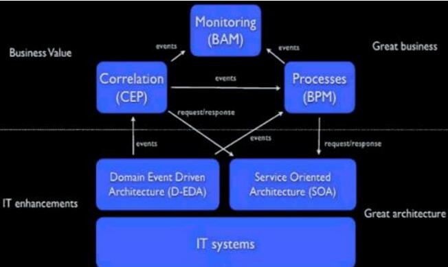
What is eda technology _eda is also called MCU
What is eda technology?