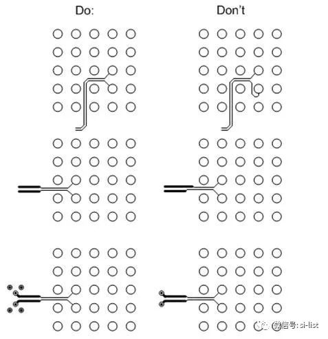
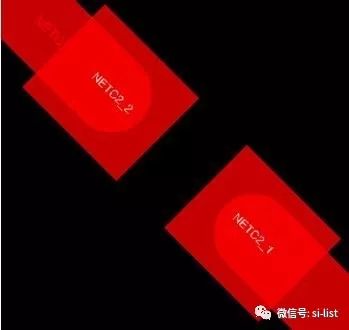
Impedance changes are affected by the following variations: wire width, spacing between adjacent wires and devices, and distance from the reference plane. However, when these changes in impedance occur on a printed circuit board (PCB), it is not always obvious. A very useful approach is to check the PCB layout or system diagram to quickly identify any problem areas that may need to be analyzed multiple times by simulation. When performing such checks, you should track the signal from the source to the receiver, look for any violations of the guidelines listed in Table 1, and the points of failure that I will discuss next. Single-ended Differential type Wire width must be constant Differential wire spacing (coupling) and wire width must be constant The spacing between wires and other devices and wires should be at least three times the wire width Constant reference plane must exist at the same distance throughout the length of the conductor Table 1: Inspection guidelines for minimizing reflections Not every time you must follow the guidelines for the transmission line in Table 1. The following are common areas where violations of these guidelines may occur: Ball Grid Array (BGA) traces—especially for multiple input/output (I/O) devices that lead to internal rows/columns. You must take extra care with the vias to ensure that a constant fixed reference plane is seen as the transmission line signal vias pass through the PCB layer. Online devices and connectors. The printed circuit board (PCB) packages of devices and connectors typically have different sizes compared to the transmission line packages that connect them, which results in impedance variations that cause reflection variations. Maintain a constant impedance by managing the trace width and the spacing of adjacent vias or pads when routing to or from the BGA device. Figure 1 shows some common considerations from the DS125DF1610 16-channel 12.5Gbps retimer data sheet (a 196-pin BGA device). Executable item Figure 1: BGA wiring rules Starting from the top, the first rule combination in Figure 1 shows you how to properly manage the differential trace collection and routing of internal BGA rows and columns. The second combination of rules highlights a common technique called necking, where it is sometimes necessary to use a smaller wire width when transmitting signals under the BGA device. The necking behavior is always performed symmetrically, where the neck length is equal to the length of the two wires of the differential pair. The third pair of combinations in Figure 1 shows one possible way to ensure that the signal vias have a constant reference plane. In this case, the "executable matter" graphic shows four arrays of ground vias arranged adjacent to the signal vias. This allows the signal to see a constant ground reference as it passes through other layers of the PCB. It is not always necessary to use 4 ground vias each time. In most cases, two ground vias are sufficient. Be sure to simulate to verify the system's needs. It is important to manage the impedance of the in-line device and connector package pads. One of the key items to look for during the inspection process is whether the package pads have any gaps or voids in the reference plane. Voids or gaps may not be necessary at a time, but if you see a significant difference between the wire width of the transfer line and the device pad, you need to investigate! Figure 2 shows an example of a wire running to a series device (in this case, a pair of AC-coupling capacitors). Figure 3 shows the ground plane below this conductor. Note the notch below the device pad, which helps to bring the impedance closer to the transmission line to reduce reflections. At the same time, Figure 4 shows the top etch and ground plane. Figure 2: Online Device Example - Signal Layer Figure 3: Example of a tandem device - ground plane Figure 4: Example of an online device - signal layer and ground plane Finally, it is necessary to perform simulations to verify your PCB layout and ensure that minimal reflections will occur. Use good practices to perform good tests and keep in mind that the guidelines in this post can help reduce simulation times and simulation time. Fog Light Wire Harness are most used in automotive,motocycle,bus,bike,truck,LVDs,medical equipment.
Yacenter has experienced QC to check the products in each process,
from developing samples to bulk, to make sure the best quality of goods. Timely
communication with customers is so important during our cooperation.
If you can't find the exact product you
need in
the pictures,please don't go away.Just contact me freely or send your sample
and drawing to us.We will reply you as soon as possible.
Fog Light Harness,Fog Light Wiring Kit,Universal Fog Light Wiring Harness,Fog Light Wiring Harness Dongguan YAC Electric Co,. LTD. , https://www.yacentercn.com


What about the distortion caused by the impedance change during the transmission? These design tips can help you
Transmission line theory tells us that the source output will not reflect any changes in the signal impedance that may be encountered between the input of the component. Essentially, when an alternating current (AC) signal encounters an impedance change as the transmission line travels down, some of the signal is reflected back to the transmitter, and the remainder of the signal will continue to hit the receiver. The greater the impedance change experienced by the signal, the greater the reflection, resulting in more signal distortion.