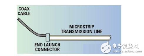
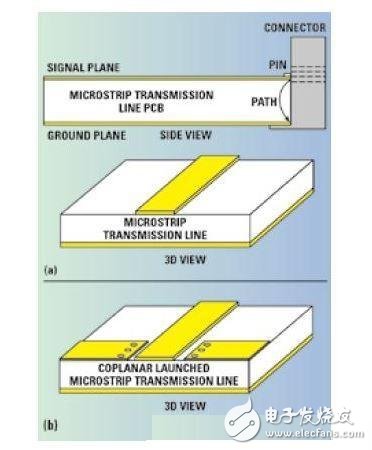
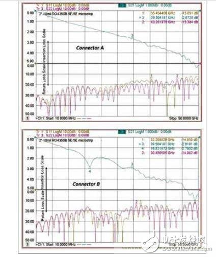
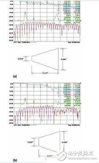
The process of transferring high frequency energy from a coaxial connector to a printed circuit board (PCB) is often referred to as signal injection, and its features are difficult to describe. The efficiency of energy transfer can vary greatly depending on the circuit structure. Factors such as PCB material and its thickness and operating frequency range, as well as connector design and its interaction with circuit materials, can affect performance. Performance can be improved by understanding the different signal injection settings and reviewing some of the RF microwave signal injection method optimization cases. Achieving effective signal injection is related to design, and general broadband optimization is more challenging than narrowband. Generally, high frequency injection is more difficult as the frequency increases, and at the same time, as the thickness of the circuit material increases, the complexity of the circuit structure increases and there are more problems. Signal injection from the coaxial cable and connector to the microstrip PCB is shown in Figure 1. The electromagnetic (EM) field distribution through the coaxial cable and connector is cylindrical, while the EM field distribution within the PCB is flat or rectangular. From one type of propagation medium to another, the field distribution changes to adapt to the new environment, creating anomalies. The change depends on the type of media; for example, signal injection is from coaxial cable and connector to microstrip, grounded coplanar waveguide (GCPW), or stripline. The type of coaxial cable connector also plays an important role. Figure 1. Signal injection from coaxial cable and connector to microstrip Optimization involves several variables. It is useful to understand the EM field distribution within the coaxial cable/connector, but the ground loop must also be considered part of the propagation medium. It is often helpful in achieving a smooth impedance transition from one propagation medium to another. Understanding the capacitive reactance and inductive reactance at impedance discontinuities allows us to understand circuit performance. If three-dimensional (3D) EM simulation is possible, the current density distribution can be observed. In addition, it is best to consider the actual situation related to radiation loss. Although the ground loop between the signal-emitting connector and the PCB may not appear to be a problem, the ground loop from the connector to the PCB is very continuous, but this is not always the case. There is usually a small surface resistance between the metal of the connector and the PCB. There is also a small difference in the electrical conductivity of the weld shop connecting the different parts and the metal of these parts. At small RF and microwave frequencies, the effects of these small differences are usually small, but the higher frequencies have a large impact on performance. The actual length of the ground return path affects the quality of the transmission that can be achieved with a given connector and PCB combination. As shown in Figure 2a, when electromagnetic wave energy is transferred from the connector pins to the signal conductors of the microstrip PCB, the ground return to the connector housing may be too long for thick microstrip transmission lines. The use of PCB materials with a higher dielectric constant increases the electrical length of the ground loop, which exacerbates the problem. Path lengthening causes problems with frequency correlation, which in turn produces local phase velocity and capacitance differences. Both are related to the impedance in the transform region and will have an effect on it, resulting in a difference in return loss. Ideally, the length of the ground loop should be minimized so that there is no impedance anomaly in the signal injection region. Note that the ground point of the connector shown in Figure 2a is only present at the bottom of the circuit, which is the worst case. Many RF connectors have ground pins that are on the same layer as the signal. In this case, the ground pad is also designed on the PCB. Figure 2b shows a grounded coplanar waveguide to microstrip signal injection circuit where the body of the circuit is a microstrip, but the signal injection region is a grounded coplanar waveguide (GCPW). Coplanar emission microstrips are useful because they minimize ground loops and have other useful features. If you use a connector with a ground pin on both sides of the signal conductor, the ground pin spacing has a significant impact on performance. This distance has been shown to affect the frequency response. Figure 2. Thick microstrip transmission line circuit and longer ground return path to the connector (a) Grounded coplanar waveguide to microstrip signal injection circuit (b). In experiments using a coplanar waveguide-transferred microstrip microstrip based on Rogers' 10 mil thick RO4350B laminate, a connector with a different coplanar waveguide grounding pitch but other similarities was used (see Figure 3). Connector A has a grounding interval of approximately 0.030" and connector B has a grounding interval of 0.064". In both cases, the connector is fired onto the same circuit. Figure 3. Testing a coplanar waveguide to microstrip circuit using a coaxial connector with similar ports with different ground spacings. The x-axis represents the frequency, 5 GHz per division. When the microwave frequency is low (< 5 GHz), the performance is equivalent, but when the frequency is higher than 15 GHz, the performance of the circuit with a large grounding interval is deteriorated. The connectors are similar, although the pin diameters of the two models are slightly different, connector B has a larger lead diameter and is designed for thicker PCB materials. This can also cause performance differences. A simple and effective signal injection optimization method is to minimize the impedance mismatch in the signal emission region. The rise in the impedance curve is basically due to an increase in inductance, while the decrease in the impedance curve is due to an increase in capacitance. For the thick microstrip transmission line shown in Figure 2a (assuming a low dielectric constant of the PCB material, about 3.6), the conductor is wider - much wider than the inner conductor of the connector. Due to the large difference in size between the circuit leads and the connector wires, a strong capacitive change occurs during the transition. Capacitive abrupt changes can often be reduced by tapering the circuit leads to reduce the size gap that is formed where they are connected to the coaxial connector pins. Narrowing the PCB lead increases its inductiveness (or reduces capacitiveity, thereby counteracting capacitive changes in the impedance curve). The effects on different frequencies must be considered. A longer gradient line will have a stronger sensibility for low frequencies. For example, if the low-frequency return loss is poor and there is a capacitive impedance spike, it is more appropriate to use a longer gradient line. Conversely, a shorter gradient line has a greater effect on high frequencies. For coplanar structures, the capacitance increases as adjacent ground planes approach. Generally, the inductive capacitance of the signal injection region is adjusted in the corresponding frequency band by adjusting the size of the gradient signal line and the adjacent ground plane spacing. In some cases, the adjacent ground pads of the coplanar waveguide are wider over a section of the gradation line to adjust the lower frequency band. Then, the pitch is narrowed in the wider portion of the gradation line, and the narrowed portion is not long in length to affect the higher frequency band. In general, narrowing the wire gradient line increases sensitivity. The length of the gradient line affects the frequency response. Changing the adjacent ground pad of the coplanar waveguide can change the capacitance, and the pad pitch can change the frequency response, which plays a major role in the change in capacitance. Instance Figure 4 provides a simple example. Figure 4a is a thick microstrip transmission line with a long and narrow gradient line. The gradient line is 0.018 (0.46 mm) wide at the edge of the board, 0.110 (2.794 mm) long, and finally becomes a 50 Ω line width of 0.064 (1.626 mm) wide. In Figures 4b and 4c, the length of the gradient line becomes shorter. The field crimpable terminal connector was selected and not soldered, so the same inner conductor was used in each case. The microstrip transmission line is 2 (50.8 mm) long and is machined on a 30 mil (0.76 mm) thick RO4350B TM microwave circuit laminate with a dielectric constant of 3.66. In Figure 4a, the blue curve represents the insertion loss (S21) with a lot of fluctuations. In contrast, S21 has the least amount of fluctuations in Figure 4c. These curves show that the shorter the gradient line, the higher the performance. Figure 4. Performance of three microstrip circuits with different gradient lines; original design with narrow and long gradient lines (a), reduced length of the gradient line (b), and length of the gradient line are further reduced (c). Perhaps the most problematic curve in Figure 4 shows the impedance of the cable, connector, and circuit (green curve). The large positive peak in Figure 4a represents the connector port 1 to which the coaxial cable is connected, and the other peak on the curve represents the connector at the other end of the circuit. The fluctuations in the impedance curve are reduced due to the shortening of the gradation line. The improvement in impedance matching is due to the widening and narrowing of the gradient line in the signal injection region; the widened gradient line reduces the inductivity. We can learn more about the size of the injected area circuit from an excellent signal injection design 2, which also uses the same plate and the same thickness. A coplanar waveguide to microstrip circuit, by using the experience of Figure 4, produces better results than Figure 4. The most obvious improvement is the elimination of the inductive peaks in the impedance curve, which is in fact caused by partial inductive peaks and capacitive valleys. Using the correct gradient line minimizes the inductive peak and uses the coplanar ground pad coupling of the implanted area to increase the inductivity. The insertion loss curve of Figure 5 is smoother than Figure 4c, and the return loss curve is also improved. For microstrip circuits using PCB materials with higher dielectric constants or different thicknesses or microstrip circuits with different types of connectors, the results of the example shown in Figure 4 are different. Signal injection is a very complex problem and is affected by many different factors. This example and these guidelines are intended to help designers understand the rationale. SSMA Cable Mount Connectors,SSMA Bulkhead Mount Connectors,SSMA Flange Mount Connectors,SSMA PCB Mount Connectors Xi'an KNT Scien-tech Co., Ltd , https://www.honorconnector.com