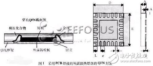
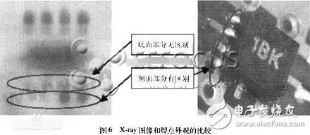
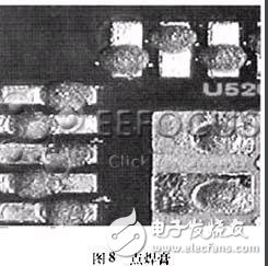
QFN (QuadFlat No-lead Package, square flat leadless package), one of the surface mount packages. Now more called LCC. QFN is the name given by the Japan Electromechanical Industry Association. The electrode contacts are arranged on the four sides of the package. Due to the absence of leads, the mounting area is smaller than QFP and the height is lower than QFP. However, when stress is generated between the printed substrate and the package, no relief can be obtained at the electrode contact. Therefore, the electrode contacts are difficult to make as many pins as the QFP, generally from about 14 to about 100. The materials are ceramic and plastic. When there is an LCC mark, it is basically a ceramic QFN. The center of the electrode contacts is 1.27 mm. Plastic QFN is a low cost package of glass epoxy printed substrate. In addition to the 1.27mm center distance of the electrode contacts, there are two types of 0.65mm and 0.5mm. Such packages are also referred to as plastic LCC, PCLC, P-LCC, and the like. The FN is a leadless package in a square or rectangular shape with a large exposed area at the center of the package for thermal conduction, and a conductive pad for electrical connection around the periphery of the package around the large pad. Because the QFN package does not have gull-wing leads like the traditional SOIC and TSOP packages, the short conductive path between the internal leads and the pads, the self-inductance coefficient and the low wiring resistance in the package provide excellent electrical performance. In addition, it provides excellent thermal performance through exposed leadframe pads, which have direct thermal pathways to dissipate heat from the package. The thermal pad is typically soldered directly to the board, and the thermal vias in the PCB help to dissipate excess power into the copper ground plane to absorb excess heat. Figure 1 shows this QFN package with exposed solder pads for PCB soldering. Due to its small size, light weight, and outstanding electrical and thermal properties, this package is ideal for any application that requires size, weight and performance. Compared with the traditional 28-pin PLCC package, the 32-pin QFN is reduced by 84% in area (5mm & TImes; 5mm), 80% in thickness (0.9mm), and 95% in weight (0.06g). Electronic package parasitics has also increased by 50%, making it ideal for high-density printed circuit boards in mobile phones, digital cameras, PDAs, and other portable small electronic devices. Standard or follow process standards (such as IPC-SM-782). Since QFN is a brand new package type, the industry standard or guide for printed circuit board pad design has not yet been developed. Moreover, after the pad design is completed, some tests are required to verify. Of course, the design principles can still be formulated with reference to the IPC method, taking into account various other factors such as the thermal pad at the bottom of the component and the tolerances of the leads and package. There are three main aspects of QFN's pad design: 1 pad design of peripheral pins; 2 design of intermediate thermal pads and vias; 3 considerations of PCB solder mask structure. Since the solder joint of QFN is under the package and the thickness is thin, X-ray can't detect less tin and open circuit of QFN solder joints. It can only be judged as much as possible by external solder joints, but currently related to QFN soldering. The criteria for determining the defect at the side of the point have not yet appeared in the IPC standard. In the absence of more methods, there will be more reliance on the test stations in the latter stages of production to judge the quality of the welds. As can be seen from the X-ray image in Fig. 6, the difference in the side portions is significant, but the image of the bottom portion that really affects the performance of the solder joints is the same, so this poses a problem for the X-ray detection judgment. With the electric iron and tin, the only increase is the side part, which has a great influence on the bottom part. X-ray still cannot judge. As seen from the partially enlarged photograph of the appearance of the solder joint, there is still a significant filling portion in the side portion. For the repair of QFN, because the solder joint is completely at the bottom of the component package, any defects such as bridging, open circuit, solder ball, etc. need to be removed, so it is somewhat similar to the BGA rework. QFNs are small, lightweight, and they are used on high-density mounting boards, making rework more difficult than BGA. At present, QFN rework is still a part of the entire surface mount process that needs to be developed and improved. In particular, it is necessary to use solder paste to form a reliable electrical and mechanical connection between the QFN and the printed board. At present, there are three possible methods of applying solder paste: one is to use a small screen printing solder paste on the PCB, and the other is to solder paste on the pad of the high-density mounting board (Fig. 8); The solder paste is printed directly on the pads of the component. All of the above methods require highly skilled reworkers to accomplish this task. The choice of rework equipment is also very important. For QFN, it is necessary to have a very good welding effect, and to prevent the components from being blown off due to too much hot air. The PCB pad design of QFN should follow the general principle of IPC. The design of thermal pad is the key. It plays the role of heat conduction. Do not cover with solder mask, but the design of via is best solder mask. When designing the stencil of the thermal pad, it is necessary to consider the release amount of the solder paste in the range of 50% to 80%. How much is appropriate, which is related to the solder mask of the via hole. The via hole during soldering is inevitable and adjusted. The temperature curve minimizes porosity. QFN package is a new type of package, which requires us to do more in-depth research from PCB design, process or inspection and repair. The QFN package (square flat leadless package) has good electrical and thermal performance, small size, light weight, and its application is growing rapidly. The QFN package with miniature lead frame is called MLF package (micro lead frame). The QFN package is somewhat similar to the CSP (Chip Size Package), but there are no solder balls on the bottom of the component. The electrical and mechanical connection to the PCB is achieved by solder paste on the PCB pad and solder joints formed by reflow soldering. Insulated Power Cable,Bimetallic Crimp Lugs Cable,Pvc Copper Cable,Cable With Copper Tube Terminal Taixing Longyi Terminals Co.,Ltd. , https://www.longyicopperlugs.com


Qfn package how to solder _qfn package soldering tutorial
What is a QFN package?