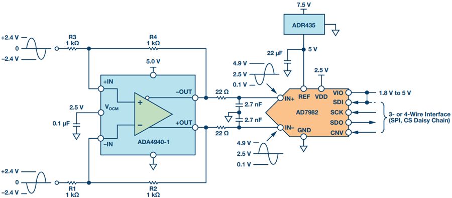
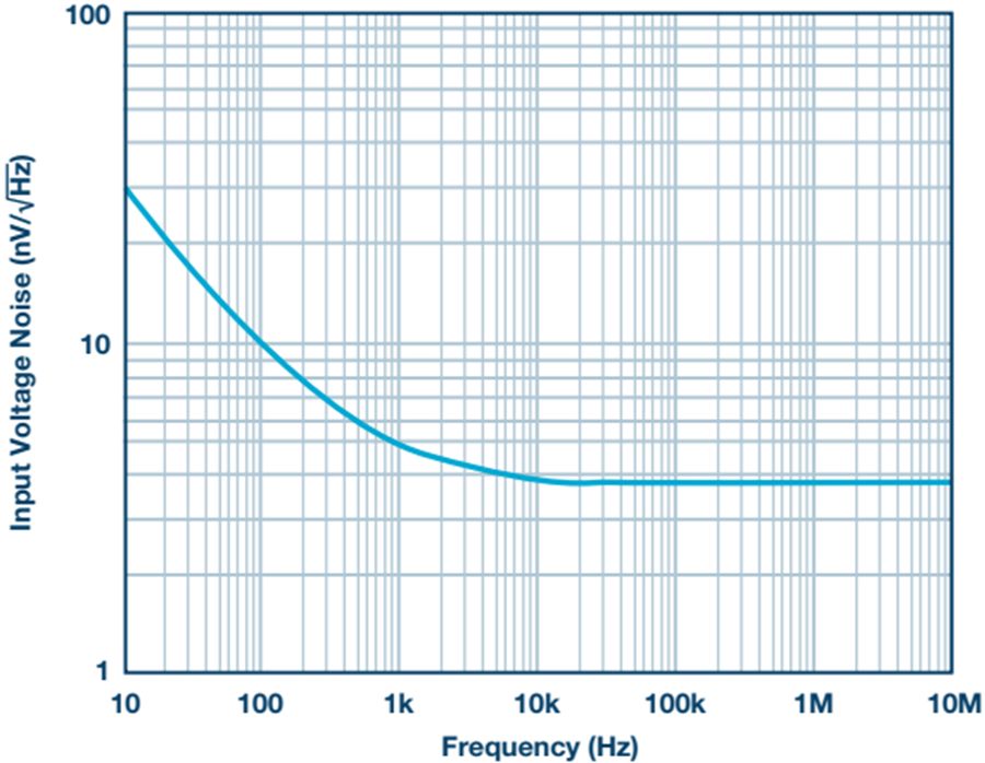
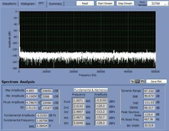
In many applications, the analog front end receives a single-ended or differential signal and performs the required gain or attenuation, anti-aliasing filtering, and level shifting, then drives the ADC input at full-scale levels. Today, we delve into the noise analysis of the precision data acquisition signal chain and study the total noise contribution of this signal chain. As shown in Figure 1, the low-power, low-noise, fully differential amplifier ADA4940-1 drives the differential input, the 18-bit, 1 MSPS PulSAR® ADC AD7982, while the low-noise precision 5 V reference ADR435 is used to provide the ADC. 5 V power supply. This signal chain eliminates the need for additional driver stages and reference buffers, simplifying analog signal conditioning, saving board space and cost. A single-pole cutoff frequency of 2.7 MHz RC (22 Ω, 2.7 nF) is placed between the ADC driver output and the ADC input to help limit ADC input noise and reduce input from successive approximation (SAR) ADCs The kickback of the end-capacity DAC. Figure 1. Low-power fully differential 18-bit 1 MSPS data acquisition signal chain (simplified schematic: all connections and decoupling are not shown). When used as an ADC driver, the ADA4940-1 allows the user to perform the necessary signal conditioning, including level shifting and attenuating or amplifying the signal to achieve a larger dynamic range with four resistors, eliminating the need for an additional driver stage. Use a feedback resistor (R2 = R4) to set the gain for the ratio of the gain resistor (R1 = R3), where R1 = R2 = R3 = R4 = 1 kΩ. For balanced differential input signals, the equivalent input impedance is 2 × gain resistor (R1 or R3) = 2 kΩ. For unbalanced (single-ended) input signals, the equivalent impedance is calculated as follows, approximately 1.33 kΩ. A termination resistor can be connected in parallel with the input if required. The internal common-mode feedback loop of the ADA4940-1 forces the common-mode output voltage to be equal to the voltage applied to the VOCM input while providing excellent output balance. When the two feedback coefficients (β1 and β2) are not equal, the differential output voltage depends on the VOCM; at this point, any imbalance in the output amplitude or phase will produce a poor common-mode component at the output, resulting in redundant noise in the differential output. And disorders. Therefore, in this case (ie, β1 = β2), the combination of the input source impedance and R1 (R3) should be equal to 1 kΩ to avoid common mode voltage mismatch of each output signal and prevent common mode of the ADA4940-1. The noise is increased. When signals are transmitted on printed circuit board (PCB) traces and long cables, system noise is added to the signal, and the differential input ADC rejects the signal noise and appears as a common-mode voltage. The expected signal-to-noise ratio (SNR) theoretical value of this 18-bit 1 MSPS data acquisition system can be calculated from the square root (RSS) of each noise source (ADA4940-1, ADR435, and AD7982). The low noise performance of the ADA4940-1 at 100 kHz is typically 3.9 nV/√Hz, as shown in Figure 2. Figure 2. ADA4940 input voltage noise spectral density versus frequency. The noise gain of the differential amplifier must be calculated to find the equivalent output noise contribution. The noise gain of the differential amplifier is: among them as well as Is the two feedback coefficients. The following differential amplifier noise sources should be considered: Since the ADA4940-1 input voltage noise is 3.9 nV/√Hz, the differential output noise should be 7.8 nV/√Hz. The common mode input voltage noise (eOCM) in the ADA4940-1 data sheet is 83 nV/√Hz, so the output noise is The R1, R2, R3, and R4 resistance noise can be calculated according to the Johnson-Nyquist noise equation for a given bandwidth condition: Where kB is the Boltzmann constant (1.38065 × 10 – 23 J/K), T is the absolute temperature of the resistance (Kelvin), and R is the resistance value (Ω). The noise from the feedback resistor is: The noise from R1 is: The noise from R3 is: The current noise in the ADA4940-1 data sheet is 0.81 pA/√Hz. Inverting input voltage noise: Non-inverting input voltage noise: Therefore, the equivalent output noise contribution from the ADA4940 is: The total integrated noise at the ADC input (after the RC filter) is: The rms noise of the AD7982 is calculated from the typical signal-to-noise ratio (SNR, 98 dB) for a 5 V reference. Based on these data, the total noise contribution of the ADC driver and ADC is Note that the noise contribution from the ADR435 reference is ignored in this example because it is very small. Therefore, the theoretical SNR of the data acquisition system can be approximated according to the following equation. The AD7982 typically has an SNR of 96.67 dB at 1 kHz input and a typical THD of –111.03 dB, as shown by the FFT performance in Figure 3. The measured SNR in this case is 96.67 dB, which is very close to the theoretical estimate of 96.95 dB SNR above. The actual loss of the target SNR of 98 dB in the data sheet is caused by the equivalent output noise contribution from the ADA4940-1 differential amplifier circuit. Figure 3. FFT plot with fIN = 1 kHz and FS = 1 MSPS (configure the ADA4940-1 as a fully differential drive). Noise is an important specification when selecting an ADC driver for a given application to drive a SAR ADC. It is also important to look at bandwidth, settling time, input/output margin/down margin, and power consumption requirements. Motor Start Switch,Single Phase Motor Starter Switches,Single Phase Centrifugal-Switches,Electric Machine Centrifugal Switch Gear Ningbo Zhenhai Rongda Electrical Appliance Co., Ltd. , https://www.centrifugalswitch.com


