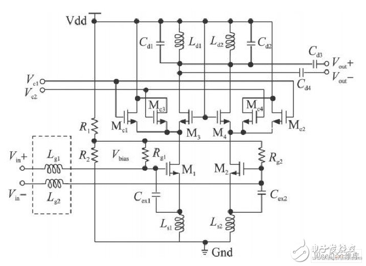
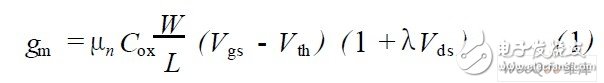
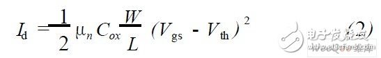
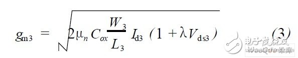
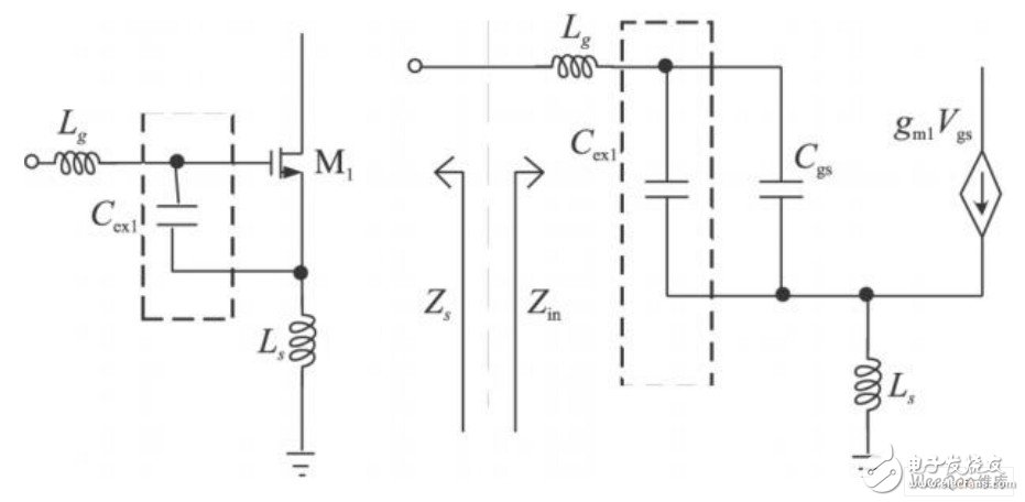
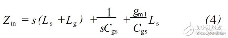
The sensor network will be the product of the fusion of information acquisition (sensing), information transmission and information processing technology. In some cases, communication cannot rely on any pre-configured network facilities, but a mobile communication technology that can temporarily and automatically organize the network. Therefore, the sensor network will gradually lead humans into the sensing era of “network or sensorâ€. The low noise amplifier (LNA) is a major component of the RF receive front end. Since the first stage at the receiving front end is directly connected to the antenna, its noise characteristics will play a decisive role in the overall system. At the same time, the signal received by the antenna is generally weak, so the low noise amplifier itself must provide enough gain to amplify the signal and transmit the useful signal to the next stage in its entirety. The low noise amplifier designed in this paper works in the 2.4 GHz band and is designed using the SM IC 0. 13μm RF CMOS process. For RF systems, especially those used in wireless sensor network nodes, power consumption is a must first consideration. On this basis, the amplifier needs to provide sufficient gain and low noise figure, and meet certain bandwidth, linearity and stability. However, it is impossible to obtain the minimum noise figure and the maximum gain at the same time. Therefore, how to achieve the best possible input and output power matching and improve the noise performance of the low noise amplifier under the premise of limiting power consumption has become the biggest challenge in the design. The circuit structure of the low noise amplifier used in this paper is shown in Figure 1. Figure 1 Schematic diagram of low noise amplifier The main circuit of the low noise amplifier adopts a cascode differential structure. Since the input impedance of the common-gate circuit is small, the voltage gain of the common source stage is suppressed, thereby suppressing the Miller effect and improving the reverse isolation. The input impedance is reduced by the gate-drain capacitance of the common source transistors M1 and M2 and the influence of the subsequent stage circuit, so that the stability of the amplifier is enhanced. In this configuration, the on-chip resistors R1, R2 are divided to generate a bias voltage Vbias, which is applied to the gates of the common source transistors M1, M2 through Rg1, Rg2 to provide a DC bias. In order to ensure a low noise figure, Rg1 and Rg2 should select a resistor with a large resistance to isolate the noise caused by the resistors R1 and R2 in the bias circuit. The transistors M3 and M4 are common gate MOS transistors. The on-chip source inductors Ls1 and Ls2 and the M1 and M2 gate-source additional capacitors Cex1 and Cex2 are matched with the gate-strip inductors Lg1 and Lg2 to achieve input matching of the low noise amplifier. The inductors Ld1 and Ld2 are connected in parallel with the capacitors Cd1 and Cd2, and are respectively connected in series with Cd3 and Cd4 to realize output matching of the low noise amplifier. The half-circuit operating state of the differential cascode amplifier shown in Figure 1 is analyzed. For MOS transistors operating in the saturation region, there are: In order to ensure that the low noise amplifier satisfies a small noise figure, the gate length of the MOS transistor in the amplifying circuit should be selected as the minimum value. The minimum gate length of the process is 0.13 μm, so the gate of the common source M1 and the common gate M3 The lengths L1 and L3 are both set to 0.13 μm. In this case, by changing the gate widths W1 and W3 of the common source and the common gate, the transconductances gm1 and gm3 of M1 and M3 can be adjusted. According to the properties of the cascode circuit, changing the transconductance of the common source and the common gate can change the gain of the amplifier. This design is powered by a 1.2 V supply voltage. To ensure a certain linearity and to ensure that the M1 gate-source voltage Vgs1 is greater than the threshold voltage Vth (the Vth of the process is approximately 430 mV), the DC bias voltage Vgs1 is selected to be 600 mV. . For a MOS transistor operating in the saturation region, its drain current Id is expressed as: This design requires a power consumption limit of 8 mW. When the bias voltage Vgs1 and various process parameters have been determined, the gate widths W1 and W3 of the common source M1 and the common gate M3 determine the operating current Id of the amplifier. That determines the power consumption of the amplifier. In the design, under the premise of ensuring the gain, adjust W1, W3, and simulate the half circuit working current is about 3 mA, that is, the total current is about 6 mA, which meets the requirements of the index. The low noise amplifier gain control circuit adopts a signal addition mode, the gain control MOS tubes Mc1, Mc2 are controlled by VC1, and Mc3, Mc4 are controlled by VC2. In the half circuit, the on and off of Mc1 can be changed by changing Vc1, and if Id1 is unchanged, the current flowing through M3 can be changed. The transconductance gm3 of the M3 tube operating in the saturation region can be expressed as: So changing Id3 can change gm3 to achieve a change in amplifier gain. The input half circuit of the low noise amplifier shown in Figure 1 and its small signal equivalent circuit are shown in Figure 2. Figure 2 Input circuit structure and small signal model First, consider the case where the input terminals are not connected to the additional capacitors Cex1 and Cex2 between the M1 and M2 gate sources. The input impedance of the amplifier is analyzed by the small-signal model of the input circuit: Twin Conductor Terminal Blocks
The JUK universal Screw Terminal Block series has the typical features which are decisive for practical applications:
l The universal foot allows the terminal blocks to be easily snapped onto the NS35 or NS32 DIN Rail with G shape.
l Closed screw guide holes ensure screwdriver operation perfect.
l For terminal block with different wire cross-sectional areas, complete accessories are available, such as end plates, partition plates, etc.
l Potential distribution achieved by fixed bridges in the terminal center or insertion bridges in the clamping space.
l Same shape and pitch Grounding Terminal Blocks as the JUK universal series.
l Adopt ZB marker strip system,achieve unified identification.
Twin Connect Terminal Block,Screw Clamp Terminal Block,Screw Type Terminal,Usb Screw Terminal Wonke Electric CO.,Ltd. , https://www.wkdq-electric.com