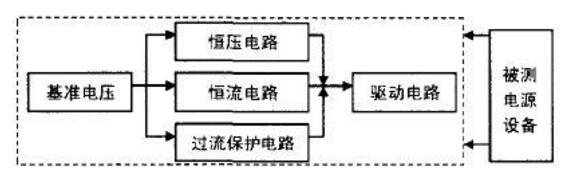
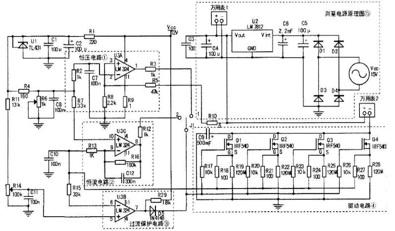
The electronic dummy load can replace the traditional load resistance box, the sliding line varistor, etc., especially the constant current or constant voltage can be set in the field that the conventional sliding line varistor cannot solve. Used for testing the output characteristics of generators, AC/DC, DC/DC converters, uninterruptible power supplies (UPS), dry batteries, batteries, transformers, chargers, etc. The maximum dummy load power is up to 600W, and the dummy load resistance can be adjusted from 30mΩ to 14.352kΩ. For power devices with electronic dummy load, FETs and IGBT tubes with small required control power are generally selected. When selecting, there must be more than the power margin at full load to avoid burnout during use; when the electronic dummy load works, a large amount of heat is generated. A heat sink needs to be installed, and the thermal resistance between the power device and the heat sink should be as small as possible. If necessary, a cooling fan can be installed; the power device of the electronic dummy load is prone to parasitic self-oscillation, and once the oscillation occurs, not only the working state is completely completed. Changed, it will also burn out the power device. Therefore, anti-parasitic self-oscillation is very important, and it is also the decisive factor for the success of electronic false load. This production produces a reference voltage that is sent to three op amps respectively, and the basic functions of the electronic dummy load are realized by constant voltage and constant current. The general principle block diagram is shown in Figure 1. Figure 1 block diagram The schematic diagram is shown in Figure 2. The basic circuit is a part other than the dotted line frame 5 and the two multimeters. It consists of a constant voltage circuit, a constant current circuit, an overcurrent protection circuit, and a drive circuit. V = 12V input voltage, after the current limiting resistor R1 to the three-terminal adjustable shunt reference source U1 (TL431) cathode K, the output reference voltage VR is 2.5V from the reference terminal R, through the resistor R1 to adjust the sliding rheostat R6, One way through the resistor R2 provides voltage for U3A, and the other through resistor R7 provides voltage for U3C. 1, constant voltage circuit As shown in Figure 2, the dotted line is shown in Figure 1. When the load input voltage increases, the U3A non-inverting input voltage increases. When the in-phase input terminal voltage is greater than the inverting input terminal voltage (reference voltage), U3A outputs a high level, and a voltage drop occurs on the gate G voltage VG of the field effect transistors Q1, Q2, Q3, Q4, so that the drain D and The voltage VDS between the sources S is reduced to achieve a constant voltage. 2, constant current circuit As shown in Figure 2, the dotted line is shown in Figure 2. As the load current increases, the voltage across R19, R22, R25, R28 increases. That is, the sampling voltage on R18, R21, R24, and R27 increases, that is, the voltage of the inverting input terminal of U3C increases. When the voltage of the inverting input terminal of U3C is greater than the voltage of the non-inverting input terminal, U3C outputs a low level, and the field effect transistor The gate G voltage VG of Q1, Q2, Q3, and Q4 decreases, and the internal resistance RDS of Q1, Q2, Q3, and Q4 increases, and the load current decreases, thereby achieving the purpose of constant current. 3, overcurrent protection circuit As shown in Figure 2, the dotted line is shown in Figure 3. When the load current increases, the voltage on R19, R22, R25, and R28 increases, that is, the sampling voltage on R18, R21, R24, and R27 increases, and the voltage at the inverting input terminal of U3B increases, but the current continues to increase. When the inverting terminal voltage is greater than the reference voltage of the set overcurrent protection current (inverting terminal input voltage), U3B outputs a low level, and the gate G voltage VG of the field effect transistors Q1, Q2, Q3, and Q4 decreases, Q1 The internal resistance RDS of Q2, Q3, and Q4 increases, and the load current decreases, thereby providing overcurrent protection. 4, the drive circuit As shown in Figure 2, the dotted line is shown in Figure 4. Q1, Q2, Q3, and Q4 use high-power FET IRF540 as the power device. However, after the multiple tubes are connected in parallel, the high-frequency characteristics of the amplifier are deteriorated due to the corresponding increase in the inter-electrode capacitance and the distributed capacitance. Frequency parasitic oscillation. For this reason, the parallel composite tubes generally do not exceed four, and an anti-parasitic oscillation resistor is connected in series to the base or the gate of each tube. R17, R20, R23, and R26 are drive resistors, R18, R21, R24, and R27 are sampled voltage resistors, and R19, R22, R25, and R28 are current limiting resistors. One end of C9 is connected to the drain of the field effect transistor IRF540, and the other end is grounded for anti-vibration. After the electronic dummy load is produced, it needs to be tested. The test circuit wiring diagram is shown in Figure 2. Dotted box 5 and two multimeter sections. The multimeter 1 measures the output voltage of the power supply, and the multimeter 2 measures the output current of the power supply. Both of the sliding resistors are hit at 50%. When the single-pole double-throw switch J1 is at the 1st end, it is in the constant voltage mode, and the output voltage of the selected power supply to be tested is kept at 12.501V, indicating that the electronic dummy load has a constant voltage function. When the single-pole double-throw switch J1 is used at the 2 terminal, it is in the constant current mode, and the output current of the selected power supply to be tested is kept at 19.993A, indicating that the electronic dummy load has a constant current function. The constant current mode can be used to test the load regulation of voltage sources and power supplies. By changing the drawing position of the slip resistor R6, the preset constant voltage current value can be changed. The preset current value of the overcurrent protection can be changed by the slip resistor R14. In the figure, the dotted box 5 is the listed measurement power supply (other power sources can also be used as the measurement power supply), V∞ is 15V AC voltage, after being rectified by the bridge rectifier circuits D1, D2, D3, D4, the capacitor is filtered to obtain DC. The voltage is regulated by the three-terminal regulator U2 (ML7812) to obtain a stable +12V DC voltage. Low Rate Nicd Battery KPL Series
Established in 1956, during the China first five-year-plan, Henan Xintaihang Power Source Co., Ltd. (Factory No.755) was the first R&D and manufacturing enterprise in China in the field of alkaline storage batteries and modular power system and it was also the military factory which owned the most varieties rechargeable batteries in domestic. Taihang was located in national Chemistry and Physicals Power Source Industrial Park, Xinxiang City, Henan, China.
Low Dishcharge Rate Nickel Cadmium Battery, KPL10~KPL1200, Max. discharge current <0.5C.
The nickel–cadmium battery (NiCd battery or NiCad battery) is a type of rechargeable battery using nickel oxide hydroxide and metallic cadmium as electrodes. The abbreviation NiCd is derived from the chemical symbols of nickel (Ni) and cadmium (Cd).
Ni Cd Battery,110V Kpl 300Ah Battery,Kpl1000Ah Nicd Battery,Low Rate Nicd Battery Kpl Series Henan Xintaihang Power Source Co.,Ltd , https://www.taihangbattery.com