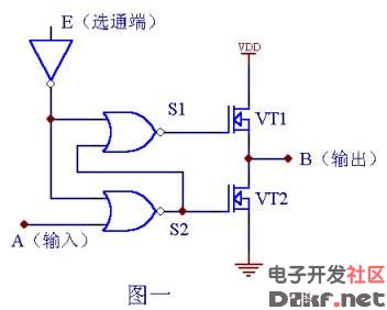
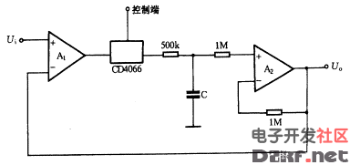
The analog switch is a tri-stable circuit that determines the state of the input and output depending on the level of the strobe. When the strobe is in the strobe state, the state of the output depends on the state of the input terminal; when the strobe is in the off state, the output is in a high impedance state regardless of the level of the input terminal. The analog switch acts primarily as a turn-on or turn-off signal in an electronic device. Because analog switches have low power consumption, high speed, no mechanical contacts, small size and long service life, they are widely used in automatic control systems and computers. First, the circuit composition and working principle of the analog switch The analog switch works as follows: When the strobe terminal E and the input terminal A are both 1, the S2 terminal is 0, and the S1 terminal is 1. At this time, VT1 is turned on, VT2 is turned off, and output B output is 1, A=B, which is equivalent to the input terminal and The output is turned on. When the strobe E is 0, and the input terminal A is 0, the S2 terminal is 1 and the S1 terminal is 0. At this time, VT1 is turned off, VT2 is turned on, and output B is 0, A=B, which is equivalent to losing. The human terminal and the output terminal are connected. When the strobe E is 0, then both VT1 and VT2 are off state, and the circuit output is in a high impedance state. It can be seen from the above analysis that the analog switch will be turned on only when the strobe terminal E is at a high level, and information can be transmitted from A to B at this time; when the input terminal A is at a low level, the analog switch is turned off. Stop transmitting information. Second, commonly used CMOS analog switch IC MOS analog switch ICs can be classified into many types depending on the characteristics of the circuit and the degree of integration. The model, name and characteristics of commonly used analog switch ICs are listed in Table 2. Third, CD4066 analog switch integrated circuit application examples The CD4066 is a bidirectional analog switch with four independent analog switches that control the transfer of digital and analog signals. Each switch has an input terminal and an output terminal, which can be used interchangeably. There is also a strobe terminal (also called a control terminal). When the strobe terminal is at a high level, the switch is turned on; when the strobe terminal is low, the strobe is low. Normally, the switch is turned off. When used, the strobe is not allowed to hang. The following are two application examples of the CD4066 analog switch. Sampling signal holding circuit The sampling signal holding circuit is shown in Figure 2. Figure 2 sampling signal holding circuit The analog signal Ui is input from the in-phase input of the operational amplifier. When the analog switch control terminal is high, the analog switch is turned on, and the capacitor C is charged to Ui. This process is called sampling of the input signal. When the sampling is finished, make the analog switch control terminal low and the analog switch open. Since the resistance of the analog switch is as high as 100M or more, and the input impedance of the operational amplifier A2 is extremely high, the sampling signal can be maintained on the capacitor C. 2. Four-way signal alternate display device A typical single-wire oscilloscope can only display one continuous signal. If this device is used, it can display four continuous signals simultaneously with a single-line oscilloscope. It is very convenient when comparing the time relationships of different signals. Pure Sine Wave Inverter,Off-Grid Pure Sine Wave Solar Inverter,Power Inverter For Solar System,Pure Sine Wave Pv Inverter Zhejiang Kaimin Electric Co., Ltd. , https://www.ckmineinverter.com