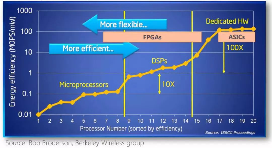
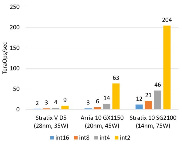
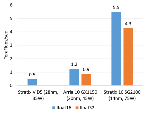
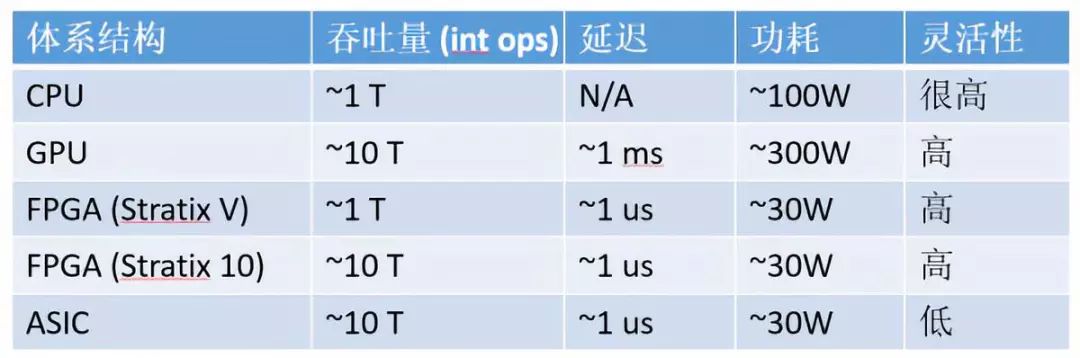
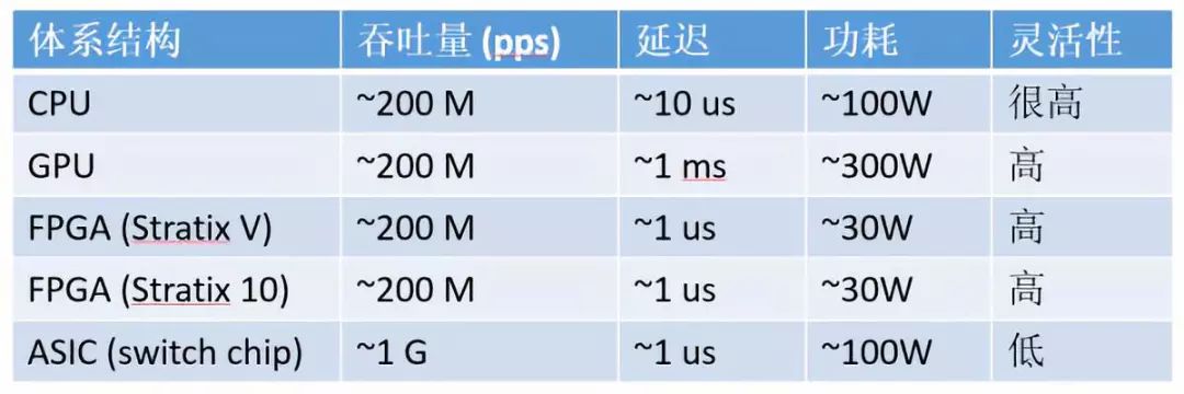
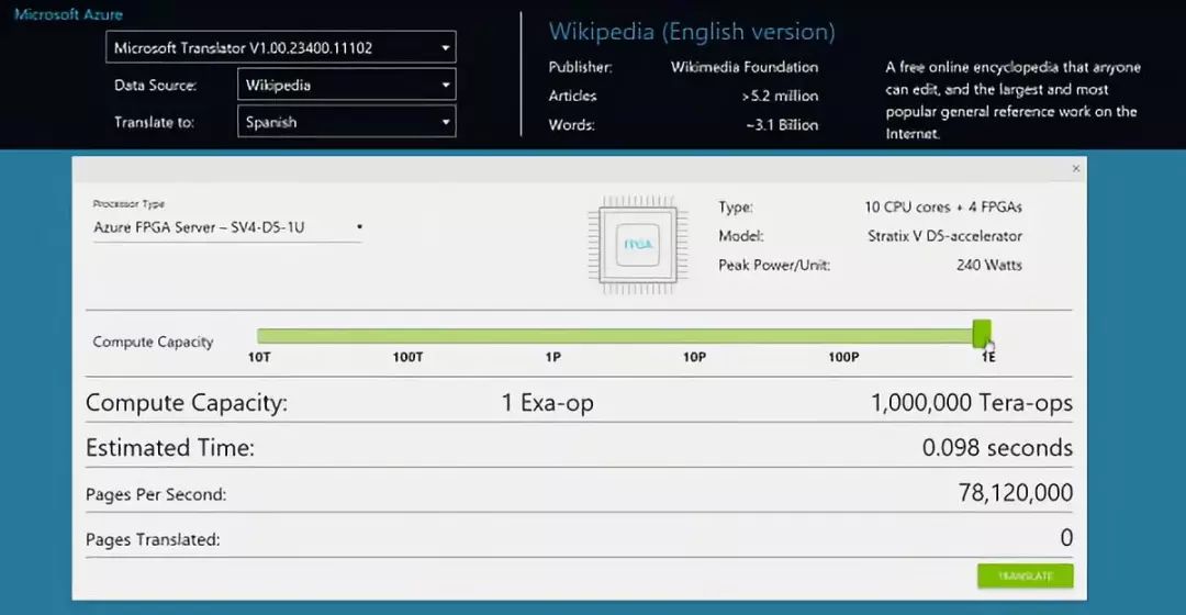
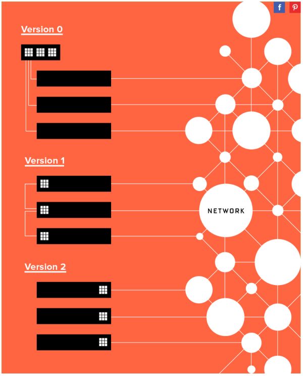
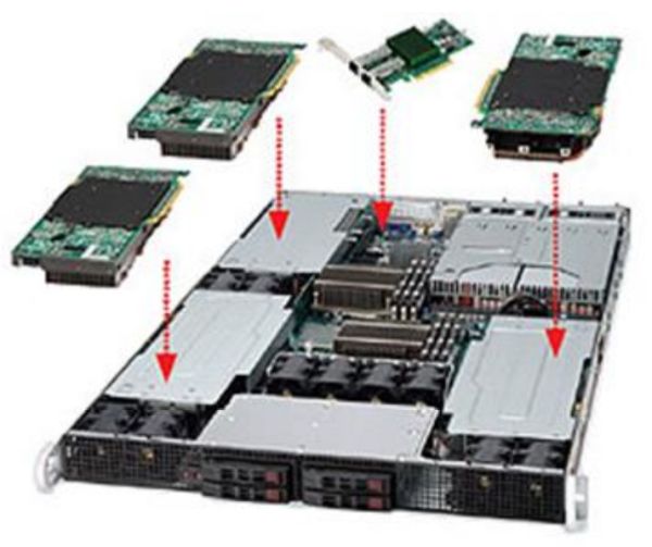
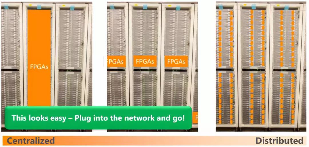
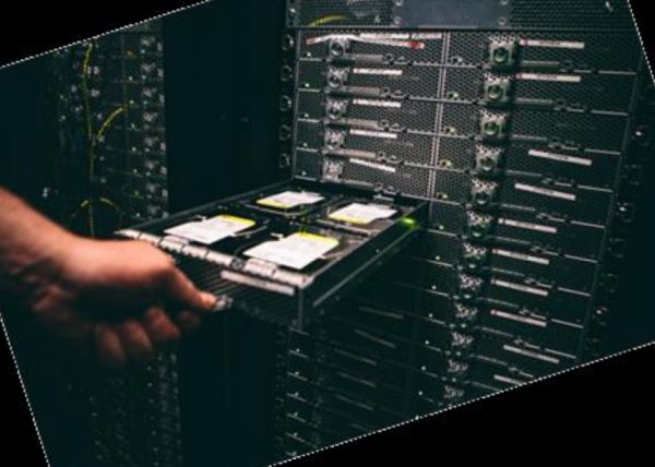
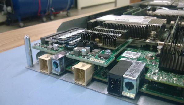
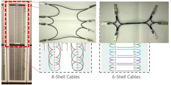
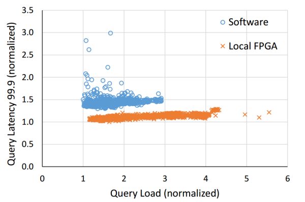
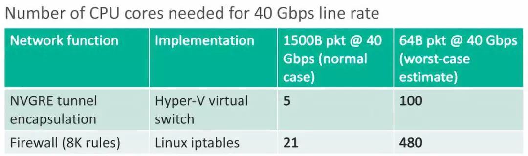
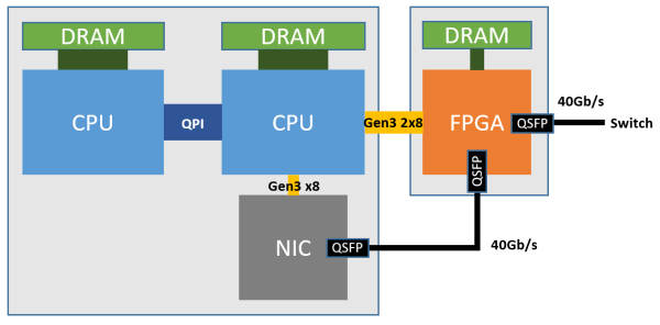
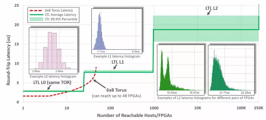
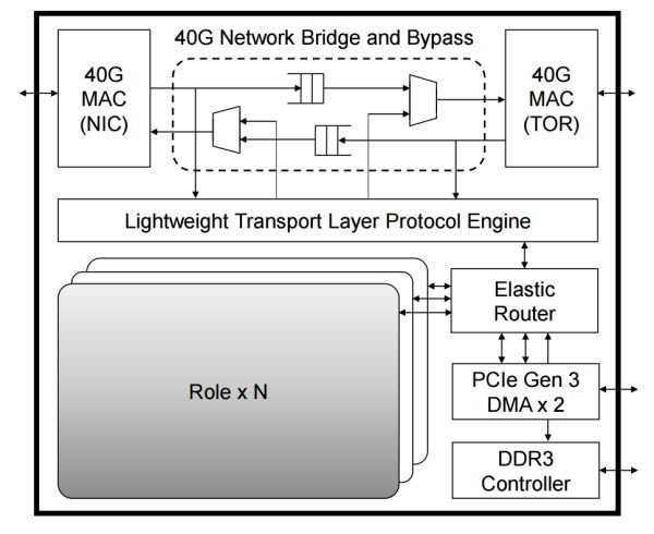
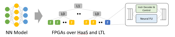
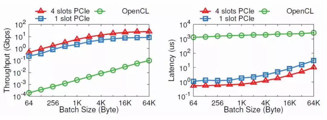
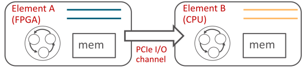
In recent years, the concept of FPGA has appeared more and more. For example, Bitcoin mining uses FPGA-based mining machines. Also, Microsoft previously stated that it will use FPGAs to "replace" CPUs in data centers, and so on. In fact, for professionals, FPGA is not new, it has been widely used. However, most people do n’t know much about it yet and have many questions about it-what exactly is an FPGA? Why use it? Compared with CPU, GPU, ASIC (dedicated chip), what are the characteristics of FPGA? ... Today, with this series of questions, let's come together to reveal FPGA. Why use FPGA? As we all know, Moore's Law for general-purpose processors (CPUs) is in its early years, while the scale of machine learning and Web services has grown exponentially. People use custom hardware to accelerate common computing tasks, but the ever-changing industry requires that these custom hardware can be reprogrammed to perform new types of computing tasks. FPGA is just a hardware reconfigurable architecture. Its full English name is Field Programmable Gate Array, and its Chinese name is Field Programmable Gate Array. FPGAs have been used as small-scale replacements for application-specific chips (ASICs) for many years, but in recent years they have been deployed in large scale in data centers of companies such as Microsoft and Baidu to provide powerful computing power and sufficient flexibility. ▲ Comparison of performance and flexibility of different architectures Why is FPGA fast? "It's all well done by colleagues." Both the CPU and GPU belong to the von Neumann structure, and the instruction decoding is executed and the shared memory is used. The reason why FPGAs are more energy efficient than CPUs or even GPUs is essentially a benefit of an architecture that has no instructions and no shared memory. In Fung's structure, since the execution unit (such as the CPU core) may execute arbitrary instructions, an instruction memory, decoder, arithmetic unit for various instructions, and branch jump processing logic are required. Because the control logic of the instruction stream is complex, there can be not too many independent instruction streams, so the GPU uses SIMD (single instruction stream multiple data stream) to allow multiple execution units to process different data at the same pace, and the CPU also supports SIMD instruction. The function of each logic unit of FPGA is already determined when reprogramming (burning), no instructions are needed. There are two roles for using memory in Feng's structure. One is to save the state, and the other is to communicate between the execution units. Since the memory is shared, access arbitration is required; in order to take advantage of access locality, each execution unit has a private cache, which must maintain the consistency of the cache between execution components. For the need to save state, the registers and on-chip memory (BRAM) in the FPGA belong to their respective control logics, without unnecessary arbitration and buffering. For the communication requirements, the connection between each logic unit of FPGA and the surrounding logic unit has been determined when reprogramming (burning), and does not need to communicate through shared memory. Having said so many 3,000 feet in height, how does the FPGA actually perform? We look at computation-intensive tasks and communication-intensive tasks separately. Examples of computationally intensive tasks include matrix operations, image processing, machine learning, compression, asymmetric encryption, Bing search ranking, etc. This type of task is usually offloaded by the CPU to the FPGA for execution. For such tasks, we are currently using Altera (it seems to be called Intel, I am still used to calling Altera ...) Stratix V FPGA's integer multiplication operation performance is basically equivalent to 20-core CPU, floating-point multiplication operation performance is 8 core The CPU is basically equivalent, but an order of magnitude lower than the GPU. The next-generation FPGA we will use, Stratix 10, will be equipped with more multipliers and hardware floating-point arithmetic components, so that it can theoretically achieve the same computing power as the current top GPU computing card. ▲ Integer multiplication capability of FPGA (estimated value, without using DSP, estimated based on logic resource occupancy) ▲ FPGA floating-point multiplication capability (estimated value, soft core for float16, hard core for float 32) In the data center, the core advantage of FPGA over GPU is latency. For tasks like Bing search sorting, to return search results as fast as possible, you need to reduce the delay of each step as much as possible. If you use GPU to accelerate, if you want to make full use of the computing power of GPU, the batch size cannot be too small, and the delay will be up to the order of milliseconds. If you use FPGA to accelerate, you only need microsecond PCIe delay (our current FPGA is used as a PCIe accelerator card). In the future, after Intel introduces Xeon + FPGA connected through QPI, the delay between the CPU and FPGA can be reduced to less than 100 nanoseconds, which is no different from accessing main memory. Why does FPGA have so much lower latency than GPU? This is essentially the difference in architecture. FPGA has both pipeline parallel and data parallel, while GPU has almost only data parallel (pipeline depth is limited). For example, there are 10 steps to process a data packet. FPGA can build a 10-stage pipeline. Different stages of the pipeline process different data packets. Each data packet is processed after 10 stages. Every time a packet is processed, it can be output immediately. The GPU data parallel method is to do 10 computing units, and each computing unit is also processing different data packets. However, all computing units must do the same thing (SIMD, Single Instruction Multiple Data) at a uniform pace. This requires that 10 data packets must be input and output together, and the input and output delay increases. When tasks arrive individually rather than in batches, pipeline parallelism can achieve lower latency than data parallelism. Therefore, FPGAs have inherent latency advantages over GPUs for streaming computing tasks. Computationally intensive tasks, orders of magnitude comparison of CPU, GPU, FPGA, ASIC (taking 16-bit integer multiplication as an example, numbers are only orders of magnitude estimation ASIC-specific chips are blameless in terms of throughput, latency and power consumption, but Microsoft did not adopt them for two reasons: The computing tasks of the data center are flexible and changeable, and the ASIC R & D cost is high and the cycle is long. Finally, a batch of accelerator cards of some kind of neural network was deployed on a large scale. As a result, another kind of neural network became more popular, and the money wasted. FPGA only needs a few hundred milliseconds to update the logic function. The flexibility of FPGA can protect investment. In fact, Microsoft's FPGA gameplay is very different from the original idea. The data center is leased to different tenants. If some machines have a neural network accelerator card, some machines have a Bing search accelerator card, and some machines have a network virtualization accelerator card, task scheduling and server operation Maintenance will be troublesome. Using FPGAs can maintain the homogeneity of the data center. Next, look at communication-intensive tasks. Compared with computationally intensive tasks, the processing of each input data by communication intensive tasks is not very complicated. Basically, the output is simply calculated, and communication will often become a bottleneck. Symmetric encryption, firewalls, and network virtualization are all examples of communication intensiveness. ▲ Communication-intensive tasks, order of magnitude comparison of CPU, GPU, FPGA, ASIC (taking 64-byte network packet processing as an example, the number is only an order of magnitude estimate) For communication-intensive tasks, FPGA has greater advantages over CPU and GPU. In terms of throughput, the transceiver on the FPGA can be directly connected to a 40 Gbps or even 100 Gbps network cable to process data packets of any size at line speed; while the CPU needs to receive the data packet from the network card to process it, many network cards cannot Wire-speed processing of small packets of 64 bytes. Although high performance can be achieved by inserting multiple network cards, the number of PCIe slots supported by the CPU and the motherboard is often limited, and the network cards and switches themselves are also expensive. In terms of latency, the network card receives the packet from the CPU and the CPU sends it to the network card. Even if a high-performance packet processing framework such as DPDK is used, the delay is 4 to 5 microseconds. A more serious problem is that the latency of general-purpose CPUs is not stable enough. For example, when the load is high, the forwarding delay may rise to tens of microseconds or even higher (as shown in the following figure); clock interruption and task scheduling in modern operating systems also increase the uncertainty of delay. ClickNP (FPGA) and Dell S6000 switch (commercial switch chip), Click + DPDK (CPU) and Linux (CPU) forwarding delay comparison, error bar means 5% and 95%. Source: [5] Although the GPU can also process data packets with high performance, the GPU does not have a network port, which means that the data packet needs to be collected by the network card first, and then the GPU does the processing. This throughput is limited by the CPU and / or network card. Not to mention the latency of the GPU itself. So why not use these network functions as network cards or use programmable switches? The flexibility of ASIC remains flawed. Although there are more and more powerful programmable switch chips, such as Tofino that supports the P4 language, ASIC still cannot do complex stateful processing, such as some custom encryption algorithm. In summary, the main advantage of FPGAs in data centers is stable and extremely low latency, which is suitable for streaming computation-intensive tasks and communication-intensive tasks. Microsoft's practice of deploying FPGA In September 2016, "Wired" (Wired) magazine published a "Microsoft bets the future on FPGA" report [3], telling the past and present of the Catapult project. Immediately afterwards, Doug Burger, the boss of the Catapult project, gave a demonstration of FPGA accelerated machine translation with Microsoft CEO Satya Nadella at Ignite 2016. The total computing power of the demonstration is 1.03 million T ops, which is 1.03 Exa-op, which is equivalent to 100,000 top GPU computing cards. The power consumption of an FPGA (plus onboard memory and network interface, etc.) is about 30 W, which only increases the power consumption of the entire server by one tenth. ▲ Demo at Ignite 2016: 1 Exa-op (10 ^ 18) machine translation computing power per second Microsoft's deployment of FPGAs has not been smooth. For the question of where to deploy the FPGA, there are roughly three stages: Dedicated FPGA cluster, filled with FPGA One FPGA per machine, using dedicated network connection One FPGA for each machine, placed between the network card and the switch, sharing the server network ▲ Three stages of Microsoft FPGA deployment The first stage is a dedicated cluster, filled with FPGA accelerator cards, like a supercomputer composed of FPGAs. The following picture is the earliest BFB experiment board. There are 6 FPGAs on one PCIe card, and 4 PCIe cards are inserted on each 1U server. ▲ The earliest BFB experiment board, placed 6 FPGAs on it. You can notice the company's name. In the semiconductor industry, as long as the volume is large enough, the price of chips will tend to the price of sand. According to rumors, it was precisely because the company refused to give the "sand price" that it chose another company. Of course, there are two companies using FPGAs in the data center field. As long as the scale is large enough, concerns about the high price of FPGAs will be unnecessary. ▲ The earliest BFB experiment board, 4 FPGA cards were inserted into the 1U server. The deployment method like a supercomputer means that there is a dedicated cabinet all of which is a server with 24 FPGAs (pictured left). There are several problems with this approach: The FPGAs of different machines cannot communicate, and the scale of problems that FPGAs can handle is limited by the number of FPGAs on a single server; Other machines in the data center have to centrally send tasks to this cabinet to form an in-cast, and network delays are difficult to stabilize. FPGA dedicated cabinet constitutes a single point of failure, as long as it is broken, no one wants to accelerate; The server equipped with FPGA is customized, and cooling and operation and maintenance both increase trouble. ▲ Three ways to deploy FPGA, from centralized to distributed. A less radical approach is to deploy a server full of FPGAs on each side of the cabinet (pictured above). This avoids the above problems (2) (3), but (1) (4) is still not resolved. In the second stage, in order to ensure the homogeneity of the servers in the data center (which is also an important reason for not using ASICs), an FPGA is inserted on each server (above right), and FPGAs are connected through a dedicated network. This is also the deployment method adopted by Microsoft in ISCA'14. ▲ Open Compute Server is in the rack. ▲ Open Compute Server interior view. The red box is where the FPGA is placed. ▲ Open Compute Server after inserting FPGA. ▲ The connection and fixation between FPGA and Open Compute Server. The FPGA uses Stratix V D5, with 172K ALMs, 2014 M20K on-chip memories, and 1590 DSPs. There is an 8GB DDR3-1333 memory, a PCIe Gen3 x8 interface, and two 10 Gbps network interfaces. The FPGA between one cabinet is connected by a dedicated network. A group of 10G network ports is connected in a group of 8 in a group, and another group of 10G network ports is connected in a group of 6 in a group, without using a switch. ▲ Network connection between FPGAs in the cabinet. Such a cluster of 1632 servers and 1632 FPGAs improves the overall performance of Bing's search result sorting by 2 times (in other words, saves half of the servers). As shown in the figure below, every 8 FPGAs are formed into a chain, and the 10 Gbps dedicated network cable mentioned above is used to communicate in the middle. These 8 FPGAs perform their duties, some are responsible for extracting features from the document (yellow), some are responsible for calculating the feature expression (green), and some are responsible for calculating the score of the document (red). ▲ FPGA accelerates the search and sorting process of Bing. ▲ FPGA not only reduces the delay of Bing search, but also significantly improves the stability of the delay. ▲ Both the local and remote FPGA can reduce the search delay. The communication delay of the remote FPGA is negligible compared to the search delay. FPGA deployment in Bing was successful, and the Catapult project continued to expand within the company. Microsoft has the most servers internally, and it is the Azure department of cloud computing. The problem that the Azure department urgently needs to solve is the overhead caused by network and storage virtualization. Azure sells virtual machines to customers and needs to provide firewall, load balancing, tunneling, NAT and other network functions to the virtual machine's network. Because the physical storage of cloud storage is separate from the computing node, the data needs to be transported from the storage node through the network, and it must be compressed and encrypted. In the era of 1 Gbps networks and mechanical hard drives, the CPU overhead of network and storage virtualization is not worth mentioning. With the faster and faster network and storage speeds, 40 Gbps on the network, the throughput of an SSD can also reach 1 GB / s, and the CPU is gradually unable to handle it. For example, the Hyper-V virtual switch can only handle about 25 Gbps of traffic, and cannot reach 40 Gbps line speed. When the data packet is small, the performance is worse; AES-256 encryption and SHA-1 signature, each CPU core can only handle 100 MB / s is only one-tenth the throughput of an SSD. ▲ The number of CPU cores required by the network tunnel protocol and firewall to handle 40 Gbps. To accelerate network functions and storage virtualization, Microsoft deployed FPGAs between network cards and switches. As shown in the figure below, each FPGA has a 4 GB DDR3-1333 DRAM, which is connected to a CPU socket through two PCIe Gen3 x8 interfaces (physically a PCIe Gen3 x16 interface, because the FPGA does not have a x16 hard core, which is logically two X8). The physical network interface card (NIC) is an ordinary 40 Gbps network interface card and is only used for communication between the host and the network. ▲ Azure server deploys FPGA architecture. FPGA (SmartNIC) virtualizes a network card for each virtual machine, and the virtual machine directly accesses this virtual network card through SR-IOV. The original data plane function in the virtual switch has been moved to the FPGA, and the virtual machine does not need the CPU to participate in sending and receiving network data packets, nor does it need to go through the physical network interface card (NIC). This not only saves CPU resources available for sale, but also improves the network performance of the virtual machine (25 Gbps), reducing the network latency between virtual machines in the same data center by 10 times. ▲ Accelerated architecture of network virtualization. Source: [6] This is the third-generation architecture of Microsoft's deployment of FPGAs, and it is also the architecture currently used for large-scale deployment of "one FPGA per server". The original intention of the FPGA multiplexing host network is to accelerate the network and storage. The far-reaching impact is to extend the network connection between FPGAs to the scale of the entire data center and make it a true cloud-scale "supercomputer." In the second-generation architecture, the network connection between FPGAs is limited to the same rack, and it is difficult to expand the scale of the interconnection between FPGAs. The forwarding through the CPU is too expensive. In the third generation architecture, FPGAs communicate with each other through LTL (Lightweight Transport Layer). Delay within 3 microseconds within the same rack; up to 1000 FPGAs within 8 microseconds; 20 microseconds to all FPGAs in the same data center. Although the second-generation architecture has lower latency within 8 machines, it can only access 48 FPGAs via the network. In order to support a wide range of inter-FPGA communication, the LTL in the third-generation architecture also supports the PFC flow control protocol and the DCQCN congestion control protocol. ▲ Vertical axis: LTL delay, horizontal axis: the number of FPGAs that can be reached. Source: [4] ▲ Logical module relationship in FPGA, where each Role is user logic (such as DNN acceleration, network function acceleration, encryption), the outside part is responsible for the communication between each Role and the communication between Role and peripherals. Source: [4] ▲ The data center acceleration plane composed of FPGA is between the network switching layer (TOR, L1, L2) and traditional server software (software running on the CPU). Source: [4] FPGAs interconnected by a high-bandwidth, low-latency network constitute the data center acceleration plane between the network switching layer and traditional server software. In addition to the acceleration of network and storage virtualization required by each server that provides cloud services, the remaining resources on the FPGA can also be used to accelerate computing tasks such as Bing search and deep neural network (DNN). For many types of applications, as the scale of distributed FPGA accelerators expands, the performance improvement is ultra-linear. For example, CNN inference, when only one FPGA is used, because the on-chip memory is not enough to put down the entire model, it is necessary to continuously access the model weights in DRAM, and the performance bottleneck is in DRAM; if there are enough FPGAs, each FPGA is responsible for one of the models Several features in the layer or layer make the model weights fully loaded into the on-chip memory, which eliminates the performance bottleneck of DRAM and fully exerts the performance of the FPGA computing unit. Of course, dismantling too thinly will also increase the communication overhead. The key to splitting tasks into distributed FPGA clusters is to balance computing and communication. ▲ From neural network model to FPGA on HaaS. Using the parallelism within the model, different layers and different features of the model are mapped to different FPGAs. Source: [4] At the MICRO'16 conference, Microsoft proposed the concept of Hardware as a Service (HaaS), that is, using hardware as a schedulable cloud service, making it possible for centralized scheduling, management, and large-scale deployment of FPGA services. ▲ Hardware as a Service (HaaS). Source: [4] From the first generation of dedicated server clusters filled with FPGAs, to the second generation of FPGA accelerator card clusters connected by private networks, to the current large-scale FPGA cloud that reuses data center networks, three ideas guide our route: Hardware and software are not a relationship that replaces each other, but a cooperative relationship; Must have flexibility, ie software-defined capabilities; Must have scalability. FPGA's role in cloud computing Finally, let me talk about my personal thinking about the role of FPGAs in cloud computing. As a third-year doctoral student, my research at Microsoft Research Asia tried to answer two questions: What role should FPGAs play in cloud-scale network interconnection systems? How to program FPGA + CPU heterogeneous system efficiently and expandably? My main regret for the FPGA industry is that the mainstream usage of FPGAs in data centers, from Internet giants other than Microsoft, to the two major FPGA vendors, and to academia, mostly regards FPGAs as computationally intensive tasks like GPUs. Accelerator card. But is FPGA really suitable for GPU? As mentioned earlier, the biggest difference between FPGA and GPU is the architecture. FPGA is more suitable for streaming processing that requires low latency, and GPU is more suitable for processing large amounts of homogeneous data. Since many people intend to use FPGA as a computing accelerator card, the high-level programming models introduced by the two major FPGA vendors are also based on OpenCL, imitating the batch processing mode of GPU based on shared memory. To do one thing for the CPU to the CPU, you need to put it into the DRAM on the FPGA board first, and then tell the FPGA to start execution. The FPGA puts the execution result back into the DRAM, and then notifies the CPU to get it back. The CPU and FPGA could have communicated efficiently through PCIe. Why do you want to go around the DRAM on the board? Perhaps it is a problem of engineering implementation. We found that it takes 1.8 ms to write DRAM through OpenCL, start the kernel, and read DRAM back and forth. Communication via PCIe DMA only takes 1 ~ 2 microseconds. The communication between multiple kernels in OpenCL is even more exaggerated. The default method is also through shared memory. At the beginning of this article, FPGAs are more energy efficient than CPUs and GPUs. The fundamental advantage of the architecture is that there are no instructions and no shared memory. Using shared memory to communicate between multiple kernels is not necessary in the case of sequential communication (FIFO). Moreover, the DRAM on the FPGA is generally much slower than the DRAM on the GPU. Therefore, we proposed the ClickNP network programming framework [5], which uses channels instead of shared memory to communicate between execution units (element / kernel), execution units and host software. Applications that require shared memory can also be implemented on the basis of pipelines. After all, CSP (Communicating Sequential Process) and shared memory are theoretically equivalent. ClickNP is still a framework based on OpenCL, and is limited by the C language to describe the hardware (of course, HLS is much more efficient than Verilog in development). The ideal hardware description language is probably not C language. ▲ ClickNP uses channel to communicate between elements, source: [5] ▲ ClickNP uses channel to communicate between FPGA and CPU, source: [5] For low-latency streaming, communication is the most important thing. However, due to the limitation of parallelism and the scheduling of the operating system, the CPU has low communication efficiency and unstable delay. In addition, communication necessarily involves scheduling and arbitration. Due to the limitation of single-core performance and the inefficiency of inter-core communication, scheduling and arbitration performance are limited. Hardware is very suitable for this kind of repetitive work. Therefore, my doctoral research defines FPGA as the "big housekeeper" of communication, whether it is server-to-server communication, virtual machine-to-virtual machine communication, process-to-process communication, and CPU to storage device. The communication can be accelerated by FPGA. Winning or losing does not matter. The lack of instructions is also the strength and weakness of FPGAs. Every time you do something different, you must occupy a certain amount of FPGA logic resources. If the things to be done are complex and not repetitive, it will occupy a lot of logic resources, most of which are idle. At this time, it is better to use the processor of von Neumann structure. Many tasks in the data center are highly localized and repetitive: one part is the network and storage that the virtualization platform needs to do, and these are all communications; the other part is the customer's computing tasks, such as machine learning and encryption and decryption. First of all, FPGA is used for the communication it is most good at. In the future, FPGA may also be leased to customers as a computing accelerator card like AWS. Regardless of communication, machine learning, encryption and decryption, the algorithm is very complicated. If you try to completely replace the CPU with FPGA, it will inevitably result in a great waste of FPGA logic resources and increase the development cost of FPGA programs. A more practical approach is that the FPGA and the CPU work together, and the locality and repeatability are attributed to the FPGA and the complexity is attributed to the CPU. When we use FPGA to accelerate more and more services such as Bing search and deep learning; when the data plane of basic components such as network virtualization and storage virtualization is controlled by FPGA; when the "data center acceleration plane" composed of FPGA becomes the network and The sky between the servers ... seems to have a feeling that the FPGA will control the whole world, and the computing tasks on the CPU will become fragmented, driven by the FPGA. In the past, we were mainly CPU-based, offloading repetitive computing tasks to the FPGA; will we become FPGA-based in the future and offload complex computing tasks to the CPU? With the advent of Xeon + FPGA, will the ancient SoC rebirth in the data center? "Across the memory wall and reach a fully programmable world." all in one energy;all in one battery,home battery,home energy storage,household power storage,home solar power,all in one system Shenzhen Enershare Technology Co.,Ltd , https://www.enersharepower.com