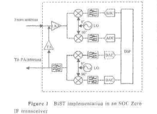
The main purpose of this article is to inspire readers to consider the impact of increased integration of electronic chips on final testing or production testing. In particular, the main transfer of radio frequency (RF) chip test methods has become increasingly feasible. Some key items about production testing will be discussed here. They are: system-level testing: RF crystal probe testing; SIP vs. SOC architecture; designer's new responsibility: RF built-in self-test (BIST); impact on test system architecture. System-level testing Modern highly integrated chips have a "RF-to-bits" or "RF-to-bits" architecture. One of the biggest impacts of the increased integration of the RF part is the transfer of test modes, which makes system-level testing possible. System-level testing has advantages and disadvantages. The biggest advantage is that it can reduce the test time. The biggest disadvantage is that it has not been widely accepted by the industry. Moreover, this is a very controversial topic. System-level testing is basically based on the function to be used by the device under test (DUT). It is very similar to go / no-go tests in digital modulation, such as bit error rate (BER) and vector error margin (EVM) tests. This test uses the signal with digital modulation information to simulate the signal received by the wireless chip at the antenna or the input signal of the wired RF chip. Traditionally, continuous wave (CW), single-tone or two-tone (Two tone) signals have been widely used for RF testing. These test methods are used because of the simple and independent RF chip structure (such as RF input and RF output). As these independent structures are integrated, the final chip structure will become crowded and complicated. Some anti-system level testers think that people cannot spend enough time in the R & D stage to consider whether all tests can guarantee to grab all the problematic parts of the chip. In order to solve this problem while ensuring the minimum test time, all of these system-level tests currently add traditional functional tests (FuncTIonal TesTIng) as supplements. As the product matures or the confidence of the design and manufacturer increases, the number of these functional tests can be gradually reduced. Another method for production testing is to make some trade-offs in a comprehensive test system-level chip [1]. That is, the system-level testing (such as BER and EVM) test as a normal production test plan, but at the same time periodically join the characterization test (CharacterizaTIon Test) plan, such as every 100 DUT. In this way, effective production testing can be guaranteed and useful information can be returned to design and manufacturing engineers. With this method, the effective test time can be defined as: For example, if the execution time of the production test obituary is 2.0 s and the characteristic test is performed for 60 s every 50 DUTs (N = 50), then the effective test time is 3.16 s. When the product is mature and requires less feedback information, you can increase the N to reduce the effective test time. If N increases to 200, then the effective test time becomes 2.29s. RF chip probe test Traditionally, especially in the field of RF testing, wafer probe testing is usually replaced by packaging testing. This is because the early design of wafer probes and wafer probe interfaces is difficult to deal with the parasitic capacitance and interface generated between the interfaces on the RF band. The inductance problem and the treatment of noise are also a big problem. However, with the emergence of SIP (System-in-a-package), the packaging is more complicated and the corresponding packaging costs have risen. ), These changes make wafer probe testing necessary. Moreover, since die with different functions are combined in one package, in the worst case, a cheap die with a low yield may damage the entire package, making the expensive die (plus package) all Useless. These requirements drive the advancement of RF wafer probe test technology. The concept of SIP also enters the category of integration. For SIP, the test can be performed after packaging or at the wafer stage before the integration of various parts. In general, before most packaging tests, each component die needs to be tested separately. For RF chips, wafer-level testing is now necessary, but in the past these tests for RF chips were avoided as much as possible. As a result, KGD has gradually made wafer probe testing of RF chips mainstream. SIP and SOC The official definition of SOC is to build a system on a single chip. However, recently, multiple dies have been introduced in one package, that is, SIP technology has been developed. In SOC chips, the core is integrated at the silicon level. In SIP, the same integration occurs at the packaging level. With the advent of SIP, different IPs (Intellectual Property) can be used in the same package. In fact, in some cases, dies from different manufacturers can also be used together. Speaking of which we must introduce a "kernel" term, the so-called kernel refers to a functional module, circuit module or separate IP. The term core has been used in traditional SOC chip design and testing for many years. This concept is a bit new for RF test engineers. This is mainly because it is only in recent independent RF chip function modules (such as low noise amplifiers, mixed Frequency converter, etc.) are placed in the same die as the digital or analog function modules. The main difference between the two integration methods of putting the RF core in the SOC or SIP is the corresponding cost benefits. These benefits can be expressed through the function of the internal use of the core. The differences between the two integration methods include: their core expectations The yield and cost of product packaging. It is like deciding whether to test each individual core or the entire SIP, which is also a function of the yield of each independent core. Considering this, the overall yield of SIP becomes the following formula: YSiP = Ycore1 & TImes; Ycore2 ×… × YcoreN Therefore, it can be clearly seen that the more cores there are in a SIP, the more the SIP's overall yield depends on the yield of individual cores in its package. Moreover, as long as there is a core with poor yield, many other good cores and the entire package will be scrapped. However, on the positive side, if the manufacturing process is well controlled and the yield is very high, when all the dies are packaged into SIP, then the cost of testing will be greatly reduced, especially when the system When the test is realized. New responsibilities of design engineers In the traditional digital test field, the final test algorithm is usually provided by the chip designer, and these algorithms are often written into the chip. Usually, designers and test engineers will not have the opportunity to cooperate in the entire product life cycle. However, with the improvement of chip integration, many things have changed. For example, designers and test engineers must work together to solve test problems. For example, in the RF field, designers must break the conventions and look forward, planning strategies and chip architectures for new production test methods. For RF, SOC, and SIP, in addition to cost and management issues, there are other factors to consider. They are: (1) How to use the engineering design and analysis tool (EDA) of the RF core to deal with the test cost problem. (2) How to actively cooperate with personnel and test engineers to create a cost-effective design for testability (DFT) architecture. (3) How to cooperate with the test development team for faster time to market. Digital core (Core) testing can be achieved using functional testing or structural testing. Over the past few years, EDA has made major advances in reducing test costs by introducing test programs into its tools to generate data compression and diagnostic capabilities. These capabilities can accelerate the time to market, reduce test time, and use low-cost test equipment. The competitive advantage of EDA's built-in self-test technology (BIST) in the digital and analog fields has increased significantly. However, it is estimated that such an advantage will disappear within a period of time after the RFBIST architecture is generally applied, which means that the RF core may become the most costly part of the SOC or SIP chip. At present, only ATE can provide some form of cost reduction in terms of integrated RF cores. In addition, the execution of parallel tests requires the support of ATE machines. Parallel testing is performed at the chip level, which takes advantage of the integration of SOC and SIP chip cores , The concept of multi-site parallel testing is extended to the multi-core (Muti-core) test of the same chip. Parallel testing requires independent access and control of the core. This independence can be controlled by the SIP chip The physical isolation of the RF core or the SOC chip enables the physical isolation of the IP core during the design stage. In SOC and SIP, when the RF core can be tested individually or in parallel with other cores, it can share the same test time with other cores with comparable test time, thereby reducing the overall test time. Parallel testing must be achieved through the cooperation of designers and test engineers. In SIP, when there is a physically isolated die, providing packaged connections does not reduce the independence of its access and control, so the parallel test application does not affect the design cycle of the chip. Test engineers only need to obtain limited information from designers to perform parallel testing. If the need for increased chip integration and reduced test costs requires designers and test engineers to communicate at a high level early in the project, then The successful application of parallel testing with separate cores and RFDFT requires more direct communication between test engineers and design engineers. Only through this communication can we understand: the benefits of parallel testing methods for reducing test time and product design changes to these designs. Requirements. Before the emergence of SOC chips, test engineers were usually assigned to a chip and required to implement all test items defined by designers or market requirements. For multi-core SOC chips, it is generally not expected that a test engineer has the ability to test all technologies in the SOC (such as RF, mixed signal, digital signal), nor does it expect that the efforts of an engineer can reach the time to market. Now, it is common for multiple engineers to work together to test a chip and apply it to the final wafer or packaging test through the integration of their different test procedures. This new organizational structure in the test field allows ATE to provide smooth test integration . RF built-in self-test technology The built-in self-test technology has been used in the design and testing of digital circuits for many years, but its application in RF circuits is still in its infancy. The purpose of the BIST test is to find defects at the transistor level, a finer level traditionally not noticed by RF test engineers. Recently, research on implementing BIST on RF chips has emerged. Figure 1 shows the architecture of a modern zero-intermediate frequency (ZIF) wireless transceiver. The integration appears in all functional modules, except for the power amplifier, the dual king device and the antenna, either on the same silicon chip or in the same package. In this example, BIST is implemented on the baseband by modulus and number The loopback test between analog-to-analog converters is implemented. Traditionally, before RF BIST was implemented, BIST technology was first implemented in the baseband section. Finally, in order to perform RF BIST, the baseband DSP sends the excitation signal to the transmit link, and then returns to the baseband signal processor for analysis through the test amplifier (TA) and the receive link. The test amplifier is turned off during the normal operation of the chip, and the impact of the test amplifier damage must be considered. In such a case, a decision must be made whether to discard the entire DUT or choose an alternative test method to retest. A typical test signal is a pseudo-random sequence generated by a baseband signal generator. The typical BIST algorithm is to generate a bit sequence, transform it and send it to the transmit link, then send it to the receive link through the test amplifier (TA), and then send it back to the baseband processor after the transform, and finally get the bit error rate BER). One disadvantage of this method is the relatively low ability to diagnose problems. For example, the reasons for the poor BER may be: the gain of the transmit link and the receive link is insufficient; the nonlinear distortion of a certain amplifier; the noise coefficient of a certain RF or mixed signal core is not good. Test system architecture With the integration of the RF part into chips that already have high-speed digital circuits and mixed-signal circuits, test systems with a single-signal scheme can no longer test such chips. In the market, there are many test systems with different functions. In addition, the market demand will also increase the integration of test machines, which will make the machines with only RF test functions disappear. In the field of automatic testing, test machines with analog, digital and RF test capabilities have emerged, just like the evolution of chip integration. The test system shown in Figure 2 was created to meet the market's wide coverage of test capabilities. It has sufficient flexibility to adapt to different market needs. in conclusion The structure of the chip and the requirement for lower test costs are changing the method of testing. In this article, we have focused on the six major changes in today. With the improvement of technical capabilities and market demand, the integration of RF into SOC (or SIP) has become a standard. Like the integration of analog, high-speed circuits and digital cores, the integration of RF makes it necessary to use the advantages of RFBIST to further reduce Test costs. At the hardware level, RF testability design (DFT) becomes valuable and ATE devices that test modern SOC chips are those that can handle multiple technologies (such as RF, mixed signal, baseband signals, memory and power management), and have the greatest And a test system with optimal parallel test capabilities. Digital scale, Weighting Scale, smart body fat scale C&Q Technology (Guangzhou) Co.,Ltd. , https://www.gzcqteq.com