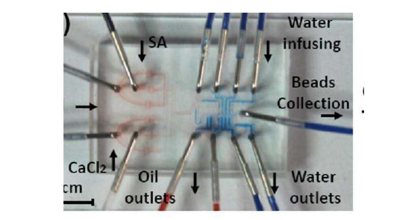
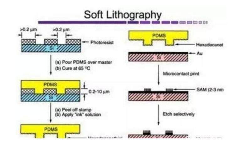
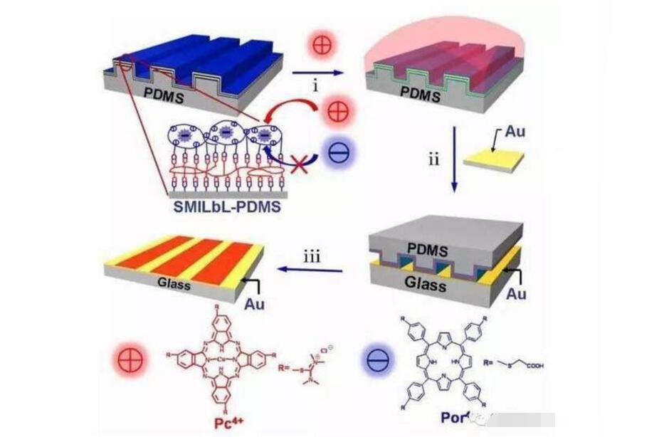
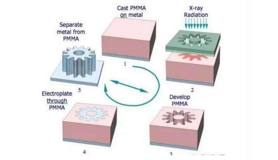
The concept of the micro total analysis system was first proposed by Manz and Widmer of Switzerland's Ciba2Geigy Corporation in 1990. At that time, it mainly emphasized the "micro" and "all" of the analysis system, and the MEMS processing method of the micro-pipeline network. Define its appearance characteristics. The following year Manz et al. achieved capillary electrophoresis and flow on a flat microchip. The current development frontier of the mini-analysis system. Microfluidic analysis systems have evolved from capillary electrophoresis separation to core analytical techniques to liquid-liquid extraction, filtration, and membrane-free diffusion. The multi-phase laminar flow separation microfluidic system has a simple structure and various separation functions, and has a wide application prospect. There have been many reports in the literature on the use of multi-phase laminar flow technology to achieve membrane-free, on-chip, sample-free, and solvent-free separations. At the same time, there are also reports of pre-processing of samples before mass spectrometry using a micro-membrane membrane dialysis machine. The flow control analysis system develops from electroosmotic flow as the main flow driving method to fluid dynamic pressure, heavy motion, centrifugal force, shear force and other means. Until today, scientists from various countries have made more remarkable achievements in this field. Microfluidic technology, as an important frontier in the current analytical science, has achieved rapid development in both research and application. The microfluidic chip adopts a semiconductor-like microelectromechanical processing technology to build a microfluidic system on a chip, and the experiment and analysis process is transferred to a chip structure composed of interconnected paths and liquid chambers, and after loading the biological sample and the reaction solution , using micro mechanical pumps. Electrohydraulic pumps, electroosmotic flow, and other methods drive the flow of buffers in the chip, form microfluidic channels, and perform one or more continuous reactions on the chip. Many detection systems such as laser-induced fluorescence, electrochemical and chemical detection systems, and mass spectrometry and other analytical methods have been used in microfluidic chips for rapid, accurate, and high-throughput analysis of samples. The most important feature of microfluidic chip is that it can form a micro total analysis system with a multi-function integrated system and a large number of composite systems on one chip. Microreactors are commonly used in microarray labs for biochemical reactions, such as capillary electrophoresis, polymerase chain reaction, enzyme reactions, and microreactors for DNA hybridization reactions. Among them, voltage-driven capillary electrophoresis (CE) is relatively easy to implement on microfluidic chips, and thus has become the fastest growing technology among them. It etched the capillary channel on the chip, and the electrophoretic sample flowed through the channel to complete the detection and analysis of the sample. If the capillary array is built on the chip, hundreds of samples can be completed in a few minutes. Parallel analysis. Since the first report of the microfluidic chip CE in 1992, progress has been rapid? The first commodity instrument is the microfluidic chip CE (Biochemical Analyzer, Aglient), which provides microfluidic chip products for nucleic acid and protein analysis. There are more and more chip-integrated unit components, and the larger the scale of integration, the greater the integration of microfluidic chips. At the same time, a large number of samples can be processed in parallel, featuring high throughput, fast analysis, low consumption, low material consumption, and low pollution. The amount of reagent required to analyze the sample is only a few microliters to several tens of microliters. The volume is even in the nano upgrade or skin upgrade. Cheap and safe, therefore, microfluidic analysis systems are miniaturized. The advantages of integrated integration and portability provide extremely broad prospects for its application in many fields such as biomedical research, drug synthesis and screening, environmental monitoring and protection, health and quarantine, forensic identification, and detection of biological reagents. Lithography is microfabrication with photoresists, masks, and UV light. The process is as follows: 1 Carefully wash the substrate; 2 The surface of a clean substrate is coated with a barrier layer such as chromium, silicon dioxide, silicon nitride, and the like; (3) A layer of several hundred A-thick photosensitive material, photoresist, is evenly thrown on the barrier layer by a squeezer. The actual thickness of the photoresist is related to its viscosity, and is inversely proportional to the square root of the spin speed of the spin-off machine; 4 Prepare the desired channel pattern on the photomask. A photomask is overlaid on the substrate, and the substrate coated with the photoresist is irradiated with ultraviolet light, and the photochemical reaction of the photoresist occurs; 5 The exposed photoresist is removed by a developing chemistry using a photoresist matching developer. In this way, the two-dimensional geometry on the film can be accurately copied to the photoresist layer by a plate making method; 6 After drying, the planar two-dimensional pattern on the film is accurately etched on the barrier layer by chemical etching using the protective effect of the unexposed photoresist. When photolithography is used to process microfluidic chips, photolithography masks must first be fabricated. There are the following requirements for the mask: 1 The contrast of light absorption or transmission between the graphic area and the non-graphic area of ​​the mask should be as large as possible; 2 Mask defects such as pinholes, broken bars, bridges, dirty spots, and bumps on lines should be minimized; The 3 masks have higher graphic accuracy. Lithographic mask materials commonly used for large scale integrated circuits are chrome plated glass plates or quartz plates coated with photo-resist. The computer graphics system is used to convert the mask image into a data file. The dedicated interface circuit is used to control the light source, the iris, the worktable and the lens in the pattern generator to make the desired pattern on the mask material. However, due to the expensive equipment, domestic research institutes need to solve the problem through external relations and delay the research cycle. Since the resolution of microfluidic chips is much lower than that of large-scale integrated circuits, it has recently been reported that simple masks and masks can be prepared using simple methods and equipment. After the micro-computer is used to convert the structure diagram of the micro-channels into image files through CAD software, The image is printed on a transparent film using a high-resolution printer. The transparent film can be used as a mask for lithography, which can basically meet the requirement of the microfluidic analysis chip for the mask. On the photo-etched substrate, the planar two-dimensional pattern on the barrier layer can be processed into a three-dimensional structure with a certain depth through wet etching and dry etching. In recent years, there have been many reports on the use of wet etching for microfabrication, which can be applied to substrates such as silicon, glass and quartz that can be corroded by chemical agents. It has been widely used in electrophoresis and chromatographic separation. The wet etching procedure is: 1 using the barrier layer protection, using a suitable etchant to etch the desired channel on the substrate; After the etching is completed, the photoresist and the barrier layer are removed, and the desired configuration of microchannels can be obtained on the substrate; 3 Drill the hole in the proper position of the substrate (generally the tip of the microchannel) as a reagent, sample, and buffer reservoir. The microfluidic substrate and the cover sheet of the same material are cleaned and bonded together under appropriate conditions to obtain a microfluidic analysis chip. For wet etching of glass and quartz, only hydrofluoric acid-containing etchant is available, such as HF/HNO3, HF/NH4. Since the etching occurs on the exposed glass surface, the deeper the channel is engraved, the greater the non-parallelism of the two walls of the channel, resulting in narrower and narrower channels. This phenomenon limits the etching of high aspect ratio channels on glass using wet methods. Plasma etching is a dry etching process based on chemical reaction. The etching gas molecules generate plasma under the action of a high frequency electric field. The free radical chemistry in the plasma is very lively. The chemical reaction between the material and the etched material is used to achieve the purpose of etching the microfluidic chip. Plasma etching has been applied to glass, quartz and silicon materials to process microfluidic chips such as quartz capillary electrophoresis and chromatography microchips. First apply a layer of positive photoresist on the quartz substrate (photopolymer after light exposure). After low-temperature drying, place a mask and develop with UV light. Microstructure images will be produced on the photoresist. The quartz substrate is then etched with active CHF3 plasma. The absence of photoresist on the substrate will produce a certain depth of channel or microstructure. This produces a high aspect ratio microstructure. Recently, there have also been reports of plasma etching used to process microchannels on polymers. Lithography and etching methods are used to make the positive mold (the desired channel part protrusions) and then cast the liquid polymer material. The cured polymer material is peeled from the positive mold to obtain a microchannel chip. This method of preparing a microchip is called a molding method. The key to molding is the choice of molds and polymer materials. The ideal materials should have low adhesion to each other and be easily demoulded. The micro-molds can be made of silicon materials, glass, epoxy SU28 negative photoresist, polydimethylsiloxane (PDMS), and the like. Through photolithography, high aspect ratio (20:1) and resolution up to several microns can be obtained on SU28 negative photoresist. After development and drying, it can be directly used as a mold; and polydimethylsiloxane can be used to mold Polydimethylsiloxane molds can be made on master molds made of materials such as silicon materials and glass. The casting polymer material should have low viscosity, low curing temperature, and can fill the microchannels and grooves on the mold under the action of gravity. There are two types of materials available: curable polymers and solvent-volatile polymers. Cured polymers include polydimethylsiloxane (silicone rubber), epoxy resin, polyurethane, etc. They are mixed with a curing agent to obtain a microfluidic chip after curing and hardening. Solvent-evolving polymers include acrylic and rubber. With fluoroplastic and the like, chips are obtained by slowly volatilizing the solvent. Although the molding method is limited to certain easily curable polymer materials, the method is simple, the chip can be copied in large quantities, does not require expensive equipment, and is a method that can make inexpensive analysis chips. However, the research on the microfluidic behavior of these microchips is still limited, and its practical value remains to be studied. Recently, several research groups led by Harvard University's Professor Whitesides research group have used self-assembled monolayers (SAMs), elastic seals, and molding of organic polymers. Based on technology, a new low-cost microfabrication technology called “soft etching†has been developed. The core of soft etching technology is the graphic transfer element - elastic stamp. The methods include microcontact printing, capillary micromolding, transfer micromolding, microreplication molding, and the like. It can not only produce complex three-dimensional microchannels on materials such as polymers, but also can change the chemical properties of the material surface. It may become a new method for producing low-cost microfluidic analysis chips. The best polymer for making an elastomeric seal is polydimethylsiloxane (PDMS). It has a low surface free energy (~21.6dyn/cm), is chemically stable, and does not adhere to other materials; it is in close contact with the substrate and is easy to take; it is soft, easy to deform, and has good elasticity. It can reproduce micropatterns on curved surfaces. . The microcontact printing method refers to a technique of printing a graphic on a flat or curved substrate by using an elastic stamp and a self-assembled monolayer technology. Self-assembled monolayers are long-chain molecules containing certain functional groups that spontaneously align to a regular structure on a suitable substrate to minimize free energy. The self-assembled monolayer systems have been determined to have alkyl mercaptans on gold and silver coinage metal surfaces and alkyl siloxanes on glass, silicon, and silica surfaces. The thickness of the self-assembled monolayer is about 2 to 3 nm. Changing the number of methylene groups in the alkyl chain can change the monolayer thickness within a precision range of 0.1 nm. Through the use of photolithography and other techniques to first prepare the mold of the graphics, PDMS can be cast on the mold to obtain an elastic stamp. The surface of the stamp is coated with an alkyl mercaptan ink to print microscopic patterns on metal surfaces such as gold and silver. In this process, the thiol molecules are automatically arranged into a regular structure to minimize the free energy and have the tendency of automatic healing defects, which can reduce print defects and ensure print clarity. The printed surface can be visualized by chemical etching or electroless plating. If the seal is made thin, it is attached to the surface of the roller and becomes a micro-printing roller, which can increase the printing efficiency and print large-area graphics. The micro-contact printing method can easily control the chemical physical properties of the micro-channel surface, and has great application prospects in the research of microfabrication, biosensors, and surface properties. Organic polymer molding methods include micro molding in capillaries (MIMIC), micro transfer molding (μTM), replica molding, and the like. In the capillary micromolding method, a capillary network is formed between the microchannel on the elastic stamp and the substrate, and a polymer prepolymer (for example, a UV-curable polyurea and a heat-cured epoxy) is dropped on the network. At the entrance, capillary action will inhale the prepolymer into the channel network. After solidification, the micro-structure complementary to the microchannel roughness on the stamp can be obtained. MIMIC can only process the micro-structure connected to the inlet and outlet of the channel network. In the micro-transfer molding method, a polymer prepolymer is filled in a groove on an elastic stamp, which is buckled on a substrate. After curing, the mold is removed, and a pattern composed of a polymer material is printed on the substrate. μTM has been used to make optical waveguides. Utilizing UV-curing polyurethane, micropipes made of μm, and pouring a cover layer on it to control the optical index difference between the waveguide and the cover by controlling the UV illumination time to control the optical coupling of the waveguide The effect is convenient and fast. The micro-replication molding method obtains a microstructure by directly pouring a polymer material such as polyurethane on an elastic stamp. This method can effectively replicate a microstructure with a size of 30 nm to a few centimeters. The surface of the polymer material is treated with oxygen plasma to modify the surface, and the obtained capillary function channel can be used for electrophoretic separation and the like. Mold-based soft etching has the advantages of simplicity, economy, and high fidelity. It can be used to process microstructures on materials such as polymers, inorganic and organic salts, sols and gels, ceramics, and carbon. Prepare micro-gratings, polymer waveguides, micro-capacitors, and micro-resonators. Photolithography can only process microstructures on polymers such as photopolymers. The polymethyl methacrylate was heated to 135° C. in a hot press, and the positive mold of silicon was held under pressure for 5 minutes under a heat preservation condition, and the microchannels could be pressed on the polymethyl methacrylate sheet. The microfluidic analysis chip can be obtained by heat sealing the substrate with the channel and the cover plate with holes. This method can be copied in large quantities, with simple equipment and easy operation. However, the materials used are limited, their performance is less studied, and the application value needs to be tested. Expose the biodegradable polymer material with a UV laser to accurately replicate the two-dimensional geometry on the film. Adjusting the exposure intensity controls the depth of photolysis of the material. A pressure purge was used to remove the degradation products, yielding a substrate with microchannels. It is thermally bonded to another well-covered cover sheet to obtain the desired chip. This method requires high technical equipment, but the procedure is simple, and it does not require a super clean environment with high accuracy. It can be used to process micro-channels on photopolymerizable materials such as polymethyl methacrylate and polycarbonate. LIGA technology is composed of three links: lithography, electroforming and plastic casting. The first step is synchrotron radiation depth X-ray burst. The pattern on the mask can be transferred to a photoresist with a thickness of several hundred microns to obtain a structure with the same mask structure with a thickness of several hundred micrometers and a minimum width of several micrometers. Three-dimensional structure. Electroforming can be electroplated. Using electroplating underneath the photoresist, the gap on the photoresist pattern is filled with metal to form a metal embossed pattern complementary to the photoresist pattern, and the photoresist and the attached base material are removed. Casting metal molds. The plastic is injected into the cavity of the metal mold through a small hole in the metal injection molding plate, and the same plastic chip as the mask structure is obtained after the press hardening. Polymethyl methacrylate is usually used as a plastic casting material. For the glass and quartz etched micro-structures, heat bonding methods are generally used. The processed substrate and the cover sheet of the same material are washed, dried, and closely aligned and placed in a high-temperature furnace, in the substrate and the cover sheet. A polished graphite plate is placed above and below, and a 0.5 Kg stainless steel block is further pressed on the upper graphite plate, and the bonding is heated in a high-temperature furnace. When the glass chip is bonded, the temperature increase rate of the high-temperature furnace is 10° C./minute, and the temperature is maintained at 620° C. for 3.5 hours, and then the temperature is lowered at a rate of 10° C./minute. Quartz chip bonding temperature up to 1000 °C or more. This method requires high operating technology. The chip can be heat-bonded multiple times if interference fringes occur after one seal. However, thermal bonding cannot be used with temperature sensitive reagents, electrodes and waveguide chips, nor can it be used for the sealing of materials with different thermal expansion coefficients. In general, sealing is more difficult than etching microstructures on glass and silicon wafers, and the rate of hot-key synthetics is not high. Anodic bonding has been widely used in the sealing of glass, quartz and silicon wafers. That is, during the bonding process, an electric field is applied so that the bonding temperature is lower than the softening point temperature. In order to prevent the possible deformation of the channel due to thermal bonding, and even the phenomenon of collapse, the anodic bonding between glass and glass has attracted widespread interest. A layer of thin film material such as polysilicon, silicon nitride, or the like is deposited on the glass surface as an intermediate layer. When the temperature is raised to 400° C. under an electric field of about 700 volts, the two glass pieces can be bonded. It has been reported in the literature that under a 500-760 volt electric field, when the temperature is raised to 500° C., two glass sheets can be bonded without depositing an intermediate layer on the glass surface. When the two glass plates are not yet bonded, the air gap between the plates assumes most of the voltage drop. The glass plate can be considered as a parallel plate capacitor. The attraction between the plates is proportional to the square of the electric field strength. Therefore, starting from the closest point in the two glasses, the positive charge (mainly Na+) in the lower plate is neutralized with the negative charge in the upper plate to form a layer of oxide. The layers make the two glass plates sealed. After the bonding is completed at this point, the surrounding air gap becomes thinner, and the electric field force increases, so that the bonding spreads out until the whole block is sealed. The glass surface is polished to reduce the gap width between the glass and the bonding temperature can be lowered. It has been reported that low-temperature bonding techniques using HF and sodium silicate bonded glass can be performed by dripping 1% HF into the gap between two glass sheets, adding 40 gf/cm2 of pressure at room temperature, and bonding can be successful in 2 hours, and the temperature rises. 60 °C high, 1h can be completed; between the two glass sheets, through the middle layer of sodium disilicate solution, placed at room temperature overnight, or placed at 90 °C for 1h can also be bonded. Sayah et al. also reported two methods of low-temperature bonding: a. Using 1 μm thick epoxy adhesive between two carefully cleaned glass sheets, hardening at 1 MPa pressure and 90°C; b. at 100-200 °C plus high pressure 15h to make direct bonding, pressure up to 50MPa.
ZGAR AZ Vape Pods 5.0
ZGAR electronic cigarette uses high-tech R&D, food grade disposable pod device and high-quality raw material. All package designs are Original IP. Our designer team is from Hong Kong. We have very high requirements for product quality, flavors taste and packaging design. The E-liquid is imported, materials are food grade, and assembly plant is medical-grade dust-free workshops.
From production to packaging, the whole system of tracking, efficient and orderly process, achieving daily efficient output. WEIKA pays attention to the details of each process control. The first class dust-free production workshop has passed the GMP food and drug production standard certification, ensuring quality and safety. We choose the products with a traceability system, which can not only effectively track and trace all kinds of data, but also ensure good product quality.
We offer best price, high quality Pods, Pods Touch Screen, Empty Pod System, Pod Vape, Disposable Pod device, E-cigar, Vape Pods to all over the world.
Much Better Vaping Experience!
Pods, Vape Pods, Empty Pod System Vape,Disposable Pod Vape Systems ZGAR INTERNATIONAL(HK)CO., LIMITED , https://www.szvape-pods.com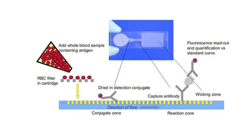
Microfluidic chip processing technology analysis
Microfluidic chip development