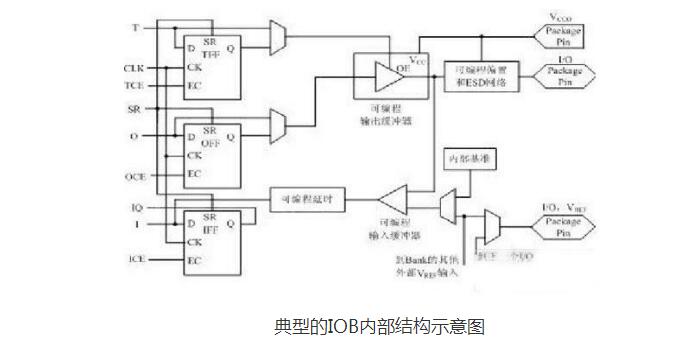
FPGA is the abbreviation of English FieldProgrammableGateArray, that is, field programmable gate array, it is in the programmable array logic PAL (ProgrammableArrayLogic), gate array logic GAL (GateArrayLogic), programmable logic device PLD (ProgrammableLogicDevice) and other programmable devices based on what is The product of further development on the FPGA. It appears as a kind of semi-custom circuit in the field of application specific integrated circuit ASIC (ApplicaTIonSpecificIntegratedCircuit), which not only solves the deficiency of custom circuit, but also overcomes the shortcomings of the limited number of original programmable device gate circuits. FPGA can complete the function of any digital device, up to high-performance CPU, down to a simple 74 series circuit, can use FPGA to achieve. FPGA is like a white paper or a pile of wood, engineers can design a digital system freely through the traditional schematic and what is the input method, or the hardware description language. Through software simulation, we can verify the correctness of the design in advance. After the completion of the PCB, it is also possible to use the on-line modification capabilities of the FPGA to modify the design at any time without changing the hardware circuit. Using FPGAs to develop digital circuits can greatly reduce design time, reduce PCB area, and increase system reliability. These advantages of PLD make PLD technology develop rapidly after 1990s, and also greatly promote the progress of Electronic Design Automation (EDA) software and Hardware-Descriptive Circuit (VHDL). FPGA has the characteristics of flexible architecture, logic unit, high integration and wide application range. Compatible with the advantages of PLDs and universal gate arrays, enabling larger scale circuits and flexible programming. Compared with other ASICs such as gate arrays, it is also widely used in products because it has the advantages of short cycle design, low manufacturing cost, advanced development tools, no need for testing of standard products, stable quality, and real-time online inspection. Prototyping and production (generally under 10,000). FPGAs can be used in almost all applications where gate arrays, PLDs, and small and medium-sized general-purpose digital integrated circuits are used FPGA adopts a new concept such as logic cell array LCA (Logic CellArray). The internal part includes configurable logic module CLB (Configurable Logic Block), output input module IOB (Input Output Block) and internal connection (Interconnect). The basic features of FPGA are: One is to use FPGA design ASIC circuit, users do not need to shoot production, you can get a shared chip. The second is that the FPGA can be used as a mid-piece for other fully custom or semi-custom ASIC circuits. The third is that there are a wealth of flip-flops and I/O pins inside the FPGA. Fourth, FPGA is one of the devices with the shortest design cycle, lowest development cost, and lowest risk in ASIC circuits. Fifth, FPGA adopts high-speed CHMOS technology, low power consumption, and can be compatible with CMOS and TTL levels. At present, the mainstream FPGA is still based on the lookup table technology, which has far exceeded the basic performance of the previous version, and integrates the hard core (ASIC type) modules of commonly used functions (such as RAM, clock management, and DSP). FPGA chip is mainly completed by 6 parts, namely: programmable input and output unit, basic programmable logic unit, complete clock management, embedded block RAM, rich wiring resources, embedded low-level functional units and embedded dedicated hardware modules . 1. Programmable Input Output Unit (IOB) Programmable input/output unit referred to as I/O unit, is the interface part of the chip and the external circuit, and completes the driving and matching requirements of the input/output signal under different electrical characteristics. In order to facilitate management and adapt to a variety of electrical standards, the FPGA IOB is divided into several banks. The interface standard of each bank is determined by its interface voltage VCCO. There can only be one type of VCCO in a bank, but the VCCO of different banks can be different. Only the ports of the same electrical standard can be connected together. The same VCCO voltage is the basic condition of the interface standard. 2. Configurable Logic Block (CLB) CLB is the basic logic unit within the FPGA. The actual number and characteristics of CLBs vary from device to device, but each CLB contains a configurable switch matrix with 4 or 6 inputs, some selector circuits (multiplexers, etc.) and flip-flops. composition. The switch matrix is ​​highly flexible and can be configured to handle combinatorial logic, shift registers, or RAM. 3. Embedded block RAM (BRAM) Most FPGAs have embedded block RAM, which greatly expands the scope of application and flexibility of the FPGA. Block RAM can be configured as common storage structures such as single-port RAM, dual-port RAM, content address memory (CAM), and FIFO. The CAM memory has a comparison logic in each internal memory cell. The data written in the CAM is compared with each internal data and returns the address of all the data with the same port data, thus the address of the route. There is a wide range of applications in the switch. In addition to the block RAM, the LUTs in the FPGA can also be flexibly configured into structures such as RAM, ROM, and FIFO. In practical applications, the amount of internal block RAM in the chip is also an important factor in selecting a chip. 4. Rich wiring resources The routing resource connects all the cells inside the FPGA, and the length and process of the connection determine the driving ability and transmission speed of the signal on the connection line. The FPGA chip has a wealth of routing resources internally and is divided into four different categories according to the process, length, width, and location of the distribution. The first type is the global routing resource, which is used for the global clock within the chip and the global reset/positioned wiring. The second type is the long-term resource used to complete the wiring between the high-speed signals of the chip Bank and the second global clock signal. The class is a short-term resource used to complete the logical interconnection and routing between basic logic units. The fourth category is distributed routing resources used for control signals such as proprietary clocks and resets. In practice, the designer does not need to directly select the routing resources, and the layout router can automatically select the routing resources according to the topological structure and constraint conditions of the input logic netlist to connect the respective module units. Essentially, there is a close and direct relationship between the use of routing resources and the design results. 5. The underlying embedded function unit The embedded function module mainly refers to soft processing cores such as a DLL (Delay Locked Loop), a PLL (Phase Locked Loop), a DSP, and a CPU. Nowadays, more and more embedded functional units make the single-chip FPGA a system-level design tool, which enables the combined design of hardware and software, and gradually transitions to the SOC platform. DLL and PLL have similar functions, can complete clock high-accuracy, low-jitter frequency multiplier and frequency division, and duty cycle adjustment and shift equal function. 6. Built-in dedicated hard core The embedded dedicated hard core refers to the soft core embedded in the bottom layer. It refers to the hard core (hardcore) with powerful FPGA processing capability and is equivalent to the ASIC circuit. In order to improve FPGA performance, chip manufacturers integrate some dedicated hard cores inside the chip. For example: In order to increase the multiplication speed of FPGA, dedicated multipliers are integrated in mainstream FPGAs; in order to apply the communication bus and interface standards, many high-end FPGAs integrate serial-serial transceivers (SERDES), which can reach tens of Gbps. Sending and receiving speed. ASIC is the abbreviation of English ApplicaTIonSpecificIntegratedCircuits, that is, application-specific integrated circuit, which refers to an integrated circuit that is designed and manufactured according to the requirements of specific users and the needs of specific electronic systems. Currently, CPLD (Complex Programmable Logic Device) and FPGA (Field Programmable Logic Array) are one of the most popular methods for ASIC design. Their commonality is that they all have user-in-field programmable features and support boundary scan technology. Both have their own characteristics in terms of integration, speed, and programming methods. ASICs are characterized by the requirements of specific users. They have many types and quantities and require short design and production cycles. They are the product of integrated circuit technology and the specific user's complete machine or system technology, and have a volume compared with general-purpose integrated circuits. Smaller, lighter weight, lower power consumption, improved performance, improved performance, enhanced privacy, reduced cost, and more. FPGA is especially suitable for sample development or small-volume product development, so that the product can be listed at the fastest speed, and when the market expands, it can be easily implemented by ASIC, so the development risk is greatly reduced. But ASIC also has its inherent advantages, the chip can get the best performance, that is, high area utilization, fast speed, low power consumption, low volume cost, so in the coming period ASIC will still occupy the high-end chip market and high-volume applications Mature low-end market. Although both FPGAs and CPLDs are programmable ASIC devices and share many common features, due to differences in the structure of CPLDs and FPGAs, they have their own characteristics: One is that the CPLD is more suitable for completing various algorithms and combinatorial logic, and the FPGA is more suitable for completing the timing FPGA logic. In other words, FPGAs are more suitable for trigger-rich structures, while CPLDs are more suitable for structures where the triggers are finite and the product terms are rich. The second is that the continuous routing structure of the CPLD determines that its timing delay is uniform and predictable, while the segmented routing structure of the FPGA determines the unpredictability of its delay. The third is that FPGA has greater flexibility than CPLD in programming. CPLDs are programmed by modifying logic functions with fixed interconnects. FPGAs are primarily programmed by changing the wiring of internal connections; FPGAs can be programmed under logic gates, and CPLDs are programmed under logic blocks. Fourth, FPGAs have higher integration than CPLDs and have more complex wiring structures and logic implementations. Fifth, CPLD is more convenient than FPGA. The programming of CPLD adopts E2PROM or FASTFLASH technology, does not need the external memory chip, it is simple to use. FPGA programming information needs to be stored in an external memory and its use is complicated. Sixth, PLD is faster than FPGA and has greater time predictability. This is due to the fact that FPGAs are gate-level programming and that CLBs use distributed interconnects, while CPLDs are logical block-level programming and the interconnections between their logic blocks are lumped. Seventh, in terms of programming, CPLD is mainly based on E2PROM or FLASH memory programming, the number of programming up to 10,000 times, the advantage is that the programming information is not lost when the system is powered off. CPLD can be divided into programming on the programmer and programming on the system. Most FPGAs are based on SRAM programming, and programming information is lost when the system is powered off. Each time the power is turned on, the programming data needs to be rewritten into SRAM from outside the device. Its advantage is that it can be programmed any number of times, and can be quickly programmed in the work, so as to realize the dynamic configuration at the board level and the system level. Eighth, the confidentiality of the CPLD is good, and the confidentiality of the FPGA is poor. Nine is the general case, CPLD power consumption is greater than the FPGA, and the higher the degree of integration is more obvious. There are three types of configuration download methods for FPGA devices: active configuration (AS), passive configuration (PS), and most commonly used (JTAG) configuration. The AS is guided by the FPGA device to configure the operating process, which controls the external memory and initialization process, the EPCS family. For example, the EPC S1 and EPCS4 configuration devices are exclusively for AS mode and currently only support the Cyclone series. Use the Altera serial configuration device to do this. Cyclone is active during the period and is subordinated during configuration. The configuration data is sent to the FPGA through the DATA0 pin. The configuration data is synchronized to the DCLK input and 1 bit of data is transmitted in 1 clock cycle. PS is controlled by an external computer or controller. This is accomplished through configuration devices such as the enhanced configuration devices (EPC16, EPC8, EPC4). During the PS configuration, the configuration data is stored externally to the FPGA through the DATA0 pin. The configuration data is latched on the rising edge of DCLK, and 1-bit data is transmitted in 1 clock cycle. The JTAG interface is an industry standard that is mainly used for chip testing and other functions. It uses IEEE Std 1149.1 combined with a boundary scan interface pin to support the JAM STAPL standard. It can be accomplished using an Altera download cable or host controller. When the FPGA is operating normally, its configuration data is stored in the SRAM and must be downloaded again when power is applied. In the experimental system, usually using a computer or controller for debugging, so you can use PS. In a practical system, in most cases, the configuration process must be actively guided by the FPGA. At this time, the FPGA will actively obtain the configuration data from the peripheral dedicated memory chip, and the fpga configuration information in this chip is the pof format that will be designed using an ordinary programmer. The file was burned into it. Dedicated Configuration Device: EPC Model Memory Commonly used configuration devices: epc2, epc1, epc4, epc8, epc1441 (now seems to have been phased out), etc. For Cyclone Cyclone II devices, ALTERA also offers configuration devices for the AS mode, EPCS series. Devices such as the EPCS1 and EPCS4 configuration devices are also serially configured. Note that they only apply to the cyclone series. In addition to single BIT configurations such as AS and PS, some devices now support parallel configuration methods such as PPS and FPS to increase the configuration speed. Of course, there are some differences between the external circuit and the PS. There are processor configurations such as JRUNNER, etc. If you need baidu again, at least no less than ten. For example, Altera's configuration methods mainly include Passive Serial (PS), Active Serial (AS), Fast Passive Parallel (FPP), Passive Parallel Synchronous (PPS), Passive Parallel Asynchronous (PPA), Passive Serial Asynchronous (PSA), JTAG, etc. Seven configuration methods, including Cyclone support configuration of PS, AS, JTAG three. 2, in the FPGA chip configuration, you can use the AS mode method, if the EPCS chip, through a download line to burn, then the beginning of 'nCONFIG, nSTATUS' should be pulled, if you consider a variety of configuration modes, Jumper design can be used. Switch the configuration mode between jumpers. The resistance of the pull-up resistor can be 10K. 3, in the PS mode tip: If you use the cable to configure the FPGA chip on the board, and this FPGA chip has a configuration chip on the board, then you must isolate the cable and configure the chip signal. (Cheung sees the figure below). In general, the configuration chip is not soldered during normal debugging. At this time, the cable is used to download the program. Only after the debugging is complete, the program is burned in the configuration chip, and then the chip is soldered. Or configure the chip that can easily remove the kind of welding. This problem can also be easily debugged. In the AS mode, tip: AS used to download a board, the configuration chip is always soldered on the board, the original AS mode when using the cable to download the configuration chip, it will automatically disable the configuration of the FPGA, and PS The method requires circuit isolation. 4, is generally used jtag configuration epc2 and flex10k, then epc2 ps configuration flex10k. This is better. (This is what I saw on the Internet. Can I use it in this way? In doubt, the watcher informs.) 5, download the cable, download cable under Altera is divided into byteblaster and byteblasterMV, and ByteBlaster II, is now also based on USB-blaster. Since BB is rarely used, and USB-Blaster is now too expensive, here to say The difference between BBII and BBMV. BBII supports multi-voltage power supply 5.5V, 3.3V, 2.5V, 1.8V; BBII supports three download modes: AS, you can program Altera's As serial configuration chip (EPCS series) PS, JTAG can be configured on the FPGA, Programmable to FPGAs, CPLDs, Altera Configuration Chips (EPC Series) and BBMVs only support PS and JTAGs 6, generally do FPGA experimental board, (such as Cyclone series), use AS + JTAG mode, so you can use JTAG debugging, and the final program has been debugged correctly, then use the AS mode to burn the program into the configuration chip Go, and there is a clear advantage, that is, when the AS mode can not be downloaded, you can use the Quartus comes with tools to generate the jic file can be used JTAG mode to verify the configuration chip is damaged. 7, Altera's FPGA can be configured through SCM, CPLD, etc., the main principle is to meet the timing of the datasheet can, here I will not say more, interested friends can look at the following articles, should be able to understand is What happened? 8, configuration, quartus software operation part: (1) Assignment--"device--"device&pin options--"Select configuration scheme, configuaration mode, configuration device, note that the configuration mode is not selectable in machines that do not support remote and local updates, and the configuration device will be based on different Configure the chip to generate a pof file. If you choose Auto, you will select the device with the lowest density and suitable design. (2) You can define the role of the dual-port pin after the configuration is completed. In the device-pin option--"dual-purpose pins--", you can continue to use the I/O port after the configuration is completed. (3) There are also many hookable options under the general menu. By default, no changes are made. For details, see alter a configuration handbook, volume2, sectionII. (4) Scope of application of files with different suffix names: sof (SRAM Object File) When using the PS mode to configure the data to be used in the FPGA, USB BLASTER, MASTERBLASER, BBII, BBMV are applicable, quartusII will Dynamic generation, all other configuration files are generated by sof. The pof (Programmer Object File) is also automatically generated by quartus II. BBII is applicable. In AS mode, the configuration data is down to the binary file that the rbf (Raw Binary File) in the configuration chip is used for the microprocessor. In the PS, FPP, PPS, PPA configuration useful rpd (Raw Programing Data File) contains the bitstream binary file, available AS mode configuration, can only be generated by the PFO file hex (hexadecimal file) This is not to say, MCU A lot of ttf (Tabular Text File) for FPP, PPS, PPA, and bit-wide PS configuration sbf (Serial Bitstream File) using PS mode configuration Flex 10k and Flex6000 jam (Jam File) dedicated program, verigy, blank -check 1. According to the role of the FPGA in the configuration circuit, configuration data can be loaded into the target device in three ways: (1) FPGA active mode: The FPGA automatically outputs the control and synchronization signals to the FPGA serial configuration chip (EPCS series). After the configuration chip receives the command, it sends the configuration data to the FPGA to complete the configuration process; in the AS mode, The FPGA must be used in conjunction with the AS serial configuration chip. The interface between the FPGA and the FPGA is four signal lines: serial clock input (DCLK), AS control signal input (ASDI), chip select signal (nCS), and string. Line data output (DATA). (2) FPGA passive mode: In the passive mode, other devices of the system initiate and control the configuration process. These devices can be configuration chips (EPC series), or single board microprocessors, CPLDs, and so on. The FPGA is completely passive during the configuration process. It only outputs some status signals to match the configuration process. In the PS mode, the clock (DCLK), configuration data (DATA0), configuration command (nCONFIG), and status signal (nSTATUS) need to be configured. The four signals of configuration completion indication (CONF_DONE) complete the configuration process. (3) JTAG mode: Configuration using JTAG can be configured using Altera's download cable, or by emulating the timing of the JTAG smart host; the JTAG interface consists of four required signals TDI, TDO, TMS, and TCK, and an optional TRST constitutes. 2. If you use the ByteBlaster II download cable, there are three supported configurations: AS mode: program the AS configuration chip (ECPS series); PS mode: The FPGA can be configured; JTAG mode: Programming of FPGAs, CPLDs, and Altera configuration chips (EPC series). 3, AS and PS mode of attention PS mode: If you use the cable to configure the FPGA chip on the board, and this FPGA chip is already equipped with the chip on the board, then you must isolate the signal from the cable and configure the chip. Normal debugging will not solder the configuration chip. , this time with cable download program. Only after the debugging is completed, the program is burned in the configuration chip, and then the chip is soldered. Or configure the chip that can easily remove the kind of welding. This problem can also be easily debugged. AS mode: AS used to download a board, the configuration chip is always soldered on the board, the original AS mode in the use of cable to configure the chip to download, will automatically disable the configuration of the FPGA, and PS mode needs Isolated on the circuit. 4, generally do FPGA experimental board, (such as Cyclone series), use AS + JTAG mode, so you can use JTAG debugging, and the final program has been debugged correctly, then use the AS mode to burn the program into the configuration chip Go, and there is a clear advantage, that is, when the AS mode can not be downloaded, you can use the Quartus comes with tools to generate the jic file can be used JTAG mode to verify the configuration chip is damaged.
A siren is a loud noise-making device. Civil defense sirens are mounted in fixed locations and used to warn of natural disasters or attacks. Sirens are used on emergency service vehicles such as ambulances, police cars, and fire trucks. There are two general types: pneumatic and electronic.
Many fire sirens (used for calling the volunteer fire fighters) serve double duty as tornado or civil defense sirens, alerting an entire community of impending danger. Most fire
sirens are either mounted on the roof of a fire station or on a pole
next to the fire station. Fire sirens can also be mounted on or near
government buildings, on tall structures such as water towers,
as well as in systems where several sirens are distributed around a
town for better sound coverage. Most fire sirens are single tone and
mechanically driven by electric motors with a rotor attached to the
shaft. Some newer sirens are electronically driven speakers.
Fire sirens are often called "fire whistles", "fire alarms", or
"fire horns". Although there is no standard signaling of fire sirens,
some utilize codes to inform firefighters of the location of the fire.
Civil defense sirens also used as fire sirens often can produce an
alternating "hi-lo" signal (similar to emergency vehicles in many
European countries) as the fire signal, or a slow wail (typically 3x) as
to not confuse the public with the standard civil defense signals of
alert (steady tone) and attack (fast wavering tone). Fire sirens are
often tested once a day at noon and are also called "noon sirens" or
"noon whistles".
The first emergency vehicles relied on a bell. Then in the 70s,
they switched to a duotone airhorn. Then in the 80s, that was overtaken
by an electronic wail.
Piezo Alarm,Siren And Alarm,Piezo Buzzer Siren,Piezo Buzzer Alarm Siren Jiangsu Huawha Electronices Co.,Ltd , https://www.hnbuzzer.com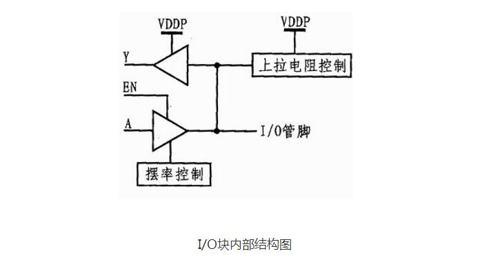
How to get from an FPGA to an expert?
FPGA Introduction