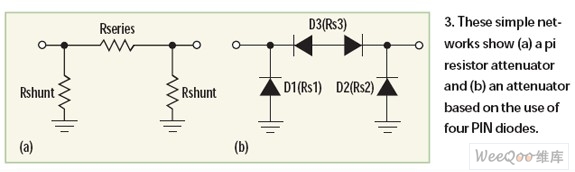
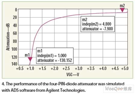
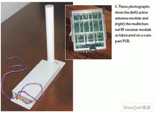
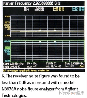
High-performance TD-SCDMA receiver design In China, Time Division Synchronous Code Division Multiple Access (TD-SCDMA), as an alternative standard for wideband CDMA (WCDMA), is trying to provide better coverage than WCDMA in various environments. WCDMA is a standard optimized specifically for symmetric services and macrocell sites. To support TD-SCDMA technology, the industry has successfully developed a compact multi-channel TD-SCDMA receiver with digital intermediate frequency (IF) level circuits and multiple active antenna modules. This smart design supports various applications in multi-carrier, diversity receiver systems. Simulation and experimental results show that this compact receiver has excellent linearity and phase-noise performance. In May 2000, the TD-SCDMA technology recommended by the China Academy of Telecommunications Science and Technology (CATT) was adopted and approved by the International Telecommunication Union (ITU) as one of the third generation (3G) mobile communication standards. TD-SCDMA has many advanced access technologies, which effectively integrate time division multiple access (TDMA), frequency division multiple access (FDMA), code division multiple access (CDMA) and space division multiple access (SDMA) methods. The uplink and downlink services in the TD-SCDMA system share the same frequency band but different time slots. Therefore, TD-SCDMA is very suitable for asymmetric data services, and can provide high spectral efficiency. The key technologies used in the TD-SCDMA system include multiplexing, smart antennas and joint detection technology. To achieve simplicity and flexibility, the intermediate frequency part of the TD-SCDMA receiver is designed with digital circuits. Compared with the standard superheterodyne receiver, its analog-to-digital converter (ADC) module is transferred to the intermediate frequency output port. By replacing analog devices with digital devices, digital intermediate frequency receivers can more flexibly handle broadband frequency ranges and multiple wireless communication standards. Receiver diversity techniques are commonly used to reduce multipath and Rayleigh fading effects that affect wireless communication performance. The main diversity techniques are frequency diversity, time diversity, antenna diversity, angle diversity and polarization diversity. TD-SCDMA receivers use antenna receive diversity technology to improve link gain. The receiver uses this method to collect multiple uncorrelated RF signals, then combine them, and reduce or even eliminate the effects of fading and multipath effects during the combining process. Typical linear diversity combining methods include selective combining (SC), maximum proportional combining (MRC), and equal gain combining (EGC). These methods have their own advantages and disadvantages. The multi-carrier technology used in TD-SCDMA can increase the data capacity and transmission rate of this format to support high data rate wireless services. Each specific cell in a multi-carrier TD-SCDMA system uses three different frequencies as carrier frequencies, one of which is called the primary frequency and the other two are called secondary frequencies. The difference between the primary frequency and the secondary frequency is whether it carries pilot and broadcast channel (BCH) information. The primary frequency needs to handle the pilot and BCH information, and the secondary frequency does not. The paging indicator channel (PICH) and the auxiliary common control physical channel (S * CH) can only be configured in the main frequency. Figure 1: The typical channel structure of a TD-SCDMA communication system uses a primary carrier and a secondary carrier. Figure 1 shows a typical TD-SCDMA radio frequency channel. This channel contains three carriers, which use the 1.28 Mchip / s chip rate which is lower than the 1.6 MHz carrier bandwidth. TD-SCDMA helps to increase the flexibility of spectrum utilization and network design, especially in densely populated areas. In addition, each TDMA frame is divided into 7 time slots within 5 ms, and these time slots can be flexibly allocated to multiple users or to a single user requiring multiple time slots. Figure 2 shows the system architecture of a multi-channel TD-SCDMA RF receiver with a digital intermediate frequency circuit and multiple active antenna modules. The system contains three active antenna modules and a radio frequency receiver module, and the latter consists of three independent radio frequency receiving channels. The active antenna module includes an omnidirectional antenna with 6dBi gain, an RF bandpass filter, and a low noise amplifier (LNA). Each channel includes a radio frequency amplifier, a down converter, a local oscillator (LO), an intermediate frequency surface acoustic wave (SAW) filter, a variable gain amplifier (VGA) controlled by a baseband processing unit, and an intermediate frequency amplifier. Figure 2: Block diagram of a TD-SCDMA RF receiver with digital IF level and multiple active antenna modules. This receiver supports multiple connection mechanisms. In the first mechanism, only one active antenna module is connected to all three channels of the receiver, and the receiver at this time is used as a multi-carrier TD-SCDMA receiver. In the second mechanism, three active antenna modules are respectively connected to the three channels of the receiver, and are used as receive diversity TD-SCDMA receivers (as indicated by the dashed arrow line in FIG. 2). In this case, the distance between the active antenna modules must be far enough to correctly receive the different propagation delays of the received signals. Usually the distance between the two antennas is at least 5 times the wavelength, so that the received signal has significantly different fading characteristics. In the third connection scheme, three active antenna modules are connected to three multi-channel RF receiver modules, which are used as diversity receivers and multi-carrier TD-SCDMA RF receivers. In order to * estimate the performance of the TD-SCDMA receiver, it is necessary to have a deeper understanding of its reference sensitivity and the function of the fast automatic gain control (AGC) circuit. The reference sensitivity is the most important indicator of the receiver. Generally speaking, it refers to the minimum input power level of the antenna port when the system reaches the required bit error rate (BER). The index is also affected by the following factors: receiver noise figure, transmitter noise floor, in-phase / quadrature (I / Q) gain imbalance, I / Q quadrature phase imbalance, local oscillator (LO) Phase noise, power supply voltage noise, linear phase distortion and linear amplitude distortion. The noise figure of the receiver and the noise floor of the transmitter show the effect of additional white Gaussian noise (AWGN), and the combined noise figure can be used to describe these two situations. In time division-duplex operation, when the receiver is turned on, the transmitter should be turned off, so the noise floor of the transmitter is not a problem for the TD-SCDMA receiver. After using digital intermediate frequency technology, the I / Q gain and phase imbalance mainly caused by the analog demodulator can be corrected in the digital domain, so it will not affect the above sensitivity index. When the local oscillator and power supply performance is high enough, the effects of phase noise and voltage noise can be ignored. Linear phase distortion and linear amplitude distortion can be compensated with a baseband processor. Based on these analyses, it can be seen that the noise figure is the main reason for the reference sensitivity of the TD-SCDMA receiver. In a conventional receiver-antenna device, the loss caused by the RF cable connecting the antenna and the RF receiver increases the noise figure of the system. In the TD-SCDMA radio frequency receiver system, the system is divided at the active antenna module, and the module is directly connected to the antenna and the low noise amplifier. Therefore, the loss caused by the RF cable can be effectively compensated, thereby improving the receiver diversity performance. When the receiver is composed of multiple blocks, each block has its own insertion gain (Gi) and noise factor (Fi). Each block adds noise to the signal, but when the signal is amplified in the previous stage circuit, the effect of subsequent blocks on the total noise factor is reduced. The noise figure of the receiver can be calculated using Equation 1. The value in Equation 1 must be calculated using the values ​​of gain and noise factor (F), not as a logarithmic noise figure value (in dB). The meaning of this simple cascaded noise figure formula is very important in system design. According to Equation 1, and considering the 3dB loss of the 5m long coaxial cable, the 1dB loss of the band-pass filter, the 1dB noise figure and 20dB gain of the low-noise amplifier, other components remain unchanged, then the noise figure can be Formula 2) is reduced to 2.14dB (Formula 3), and the reference sensitivity of the TD-SCDMA receiver has been significantly improved. The AGC circuit used in the receiver can provide a constant level signal to the ADC. AGC attenuators based on PIN diodes are often used in many broadband system applications such as WiMAX and 3G cellular systems. TD-SCDMA receivers often use the digital AGC method without analog circuits to provide flexible and consistent performance. The PIN diode attenuator is used for analog attenuation in each RF channel and is controlled by the digital baseband circuit. For common attenuation values, the resistance value is 50Ω. According to the π resistance attenuator block diagram, four PIN diodes are used in the circuit shown in Figure 3 (b). In the switching circuit, the resistance characteristics of the maximum and minimum points of the PIN diode are fully utilized. However, the limited value of PIN diode resistance is used in the attenuator. The advantage of this circuit is its symmetry, which allows the use of a relatively simple bias network, and because the harmonic signals in such back-to-back connected serial diode circuits can cancel each other and reduce distortion. Although there are other methods to provide AGC functions, such as changing the gain of the RF transistor amplifier, the PIN diode method usually has the characteristics of low power consumption, broadband constant impedance, wide dynamic range, low frequency traction and high linearity. Figure 3: (a) Typical π-type resistance attenuator; (b) PIN attenuator. Figure 4: Using Agilent's ADS software to simulate an attenuator consisting of 4 PIN diodes. Using the Advanced Design System (ADS) software tool suite provided by Agilent Technologies, a computer simulation of the PIN diode attenuator used in the above AGC circuit was performed. The dynamic range results obtained by simulation are shown in Figure 4. The dynamic range obtained from these simulations can reach 120dB. Although the attenuation curve is not linear, the AGC control voltage can be corrected by the baseband algorithm to achieve an effective linear response. Compared with the traditional loop-type AGC circuit, this digital AGC technology is faster and more suitable for TDD systems. Figures 5 (a) and 5 (b) are the active antenna module and multi-channel RF receiver module, respectively. This multi-channel RF receiver module is integrated on a four-layer circuit board with a size of 150x200x20mm. Figure 6 shows the overall receiver noise figure measured with Agilent Technologies 'N8975A noise figure analyzer and the modulation performance also measured with Agilent Technologies' E4438C signal generator and 89600 software. As shown in Figure 6, the receiver noise figure is less than 2dB, and the reference sensitivity measured by the system is -115dBm. Figure 7 shows the error vector magnitude (EVM) performance.
Portable Monitor Holder For Laptop,Adjustable Portable Laptop Holder,Adjustable Ergonomic Portable Aluminum Laptop Holder,Foldable Portable Desktop Laptop Holder,etc.
Shenzhen Chengrong Technology Co.ltd is a high-quality enterprise specializing in metal stamping and CNC production for 12 years. The company mainly aims at the R&D, production and sales of Notebook Laptop Stands and Mobile Phone Stands. From the mold design and processing to machining and product surface oxidation, spraying treatment etc ,integration can fully meet the various processing needs of customers. Have a complete and scientific quality management system, strength and product quality are recognized and trusted by the industry, to meet changing economic and social needs .
Portable Monitor Holder For Laptop,Adjustable Portable Laptop Holder,Adjustable Ergonomic Portable Aluminum Laptop Holder,Foldable Portable Desktop Laptop Holder Shenzhen ChengRong Technology Co.,Ltd. , https://www.chengrongstand.com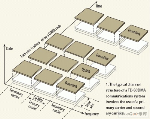
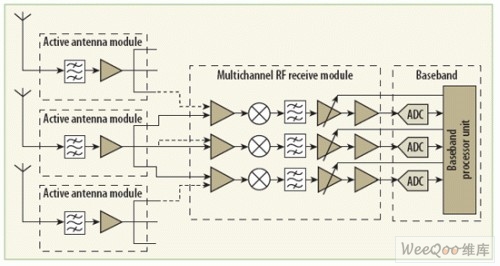

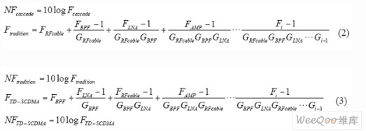
Figure 3 (a) is a typical π-type resistance attenuator, whose attenuation is determined by Equation 4, where the parameter K is defined as the input-to-output voltage ratio, and Z0 represents the system characteristic impedance.