0 Preface This article refers to the address: http:// Shenzhen Guan Chen Electronics Co., Ltd. is a High-tech enterprise that
integrates R&D, design, manufacture of computer peripheral products.The
products include Thunderbolt Docking Station,USB Docking Station,USB Hubs,USB
Adapter, Thunderbolt Cable , SSD Enclosure , HDD Enclosure . Our company adheres to
the principle and motto of Being sincere, Responsible, Practical to meet the
needs of markets and customers with high quality technology and management. We
commit ourselves to new product development and also stress the exploring of
international markets.
Our company owns a professional production team and establishes strict
quality control standard, so we can provide high quality products and service
for customers. We have Grapgic designer,3D Deisnger and Electronic designer to
provides professional OEM/ODM service. Our factory covers an area of 1,000-2000
spare meters, which houses 100-200 workers, so our production capacity reaches
50,000 pieces every day.With more than 10 engineers focusing on research and
development, our private model attracts much among different markets. Over 100
new designed models are released per year.There are also 3 lean production
lines to fullfill small quatity orders production for variety of models.
Our Thunderbolt 3 Docking Station has passed thunderbolt certified by
intel and apple.Our product also all can meet with CE, RoHS, UL, FCC and other
related certification.And our factory also meets legal environmental standards
ensuring your order is delivered. We have a very good reputation at home and
abroad. Our products are mainly exported to Europe, USA and Southeast Asia. We
provide one-stop-service and promote customers achieve rapidly development.
Customer comes First, Quality Ranks First, and Reasonable Price.Guanchen will
be your faithful partner from China.
Usb To Usb Adapter,100W Usb To Usb Adapter,Usb C Hub 6-In-1 Adapter,Enclosure Usb Adapter Shenzhen GuanChen Electronics Co., Ltd. , https://www.gcneotech.com
The digital responder control system plays an irreplaceable role in various knowledge contests held by many factories, schools and TV stations. The electronic responder designed based on EDA technology has been widely welcomed by its low price, safe and reliable, and convenient to use. In this paper, the field programmable logic device (FPGA) is used as the design carrier, and the hardware description language VHDL is the main expression. The electronic answering device designed by OuartusII development software and GW48EDA development system is designed to have the function of answering and discriminating and latching. The second-question time limit function, the warning group for the foul response, and the corresponding score addition and subtraction operations for each answering group.
1 Function of the electronic responder The functions implemented by the electronic responder mainly include four operations:
(1) Identification and latching of the first rushing signal The electronic acknowledgment device has four groups, each of which controls one rushing switch, which are a, b, c, and d, respectively. After the host issues a response command, if the contestant presses the responder button, the group indicator lights up and the display shows the group of the responder. At the same time, the circuit is in a self-locking state so that the other groups of responder buttons do not work.
(2) Timing function In the initial state. The host can set the initial value of the answer time. After the host confirms the rushing group and gives a countdown start signal, the responder can begin to answer the question. At this time, the display counts down from the initial value, counts to 0 to stop counting, and the speaker emits a timeout alarm signal. If the contestant answers the question within the specified time, the host can give a timing stop signal to prevent the speaker from beeping.
(3) Scoring function In the initial state, the moderator can set an initial score for each group. After each group is answered, the host will score, and the answer will be increased by 1 point, and the wrong answer will be reduced by 1 point.
(4) Foul setting A beep warning is given to the early responder and the overtime responder, and the foul group is displayed.
2 The structure principle of the electronic responder
2.1 The overall structure of the electronic responder The overall structure of the electronic responder is shown in Figure 1. It includes an authentication and latching module, a timing and foul setting module, and a scoring module. 
2.2 Identification and Latching Module Design The main function of the authentication and latching module is to judge the order of the four groups of a, b, c, and d, record the group number that is the first to answer, and no longer accept other The signal is input, and the group that is the first to answer is latched, and the group that is the first to answer is displayed.
According to the above functional requirements, the source program of the module must contain four answer input signals. Now set its signal to a, b, c, d respectively; when answering, you must have a signal to allow the start of the answer, set its signal to sta, after the signal is input, its output indicator lights, so that the player knows that the allowed signal has been Is issued, so you can set the output indicator signal of a sta as star-t; in order to identify the first responder, you can set the output indicators of group a, b, c, d to led_a, led_b, led_c, led_d, and set The output signal showing the first answer group number is states[3. . 0]; In order to put the system into the re-answer state, you also need to set a system reset signal, which can be set to rst. The simulation waveform of the identification and latch module is shown in Figure 2.
It can be seen from Figure 2 that when rst=1, the system is in the initial state, at this time all inputs are invalid; when rst=O and sta=O, the answer is invalid; and when rst=O and sta=1, start The indicator light is on, the d group is the first effective answering group, the led_d indicator is on, and the d group of the successful reply group is “0100â€. Through the simulation diagram and analysis of Fig. 2, it can be seen that the function of the identification and latching module is correctly designed. 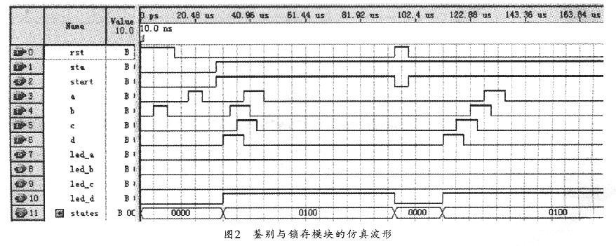
2.3 Electronic Responder Timing and Offense Block Design The main function of timing and offense block is to limit the time limit. When the countdown time is counted as 0, the system will output an alarm signal to give a beep alert to the early responder and display the foul group number.
According to the above functional design requirements, the module needs to set a down counter to limit the answer time, and its signal can be set to time[7..0]. In order to enable the countdown timer to start or stop working, a timing enable input signal en should be set; in order to determine whether a player has answered in advance or overtime, the allowable answer signal sta and four answer inputs (a, b, c, d) ), display the success of the group of groups [3. . 0], the system clock signal clk_1hz, etc. as the input signal, and the foul alarm signal alarm and the foul group display offender as the output signal. In order to stop the buzzer or cause the system to re-enter the active rush state, the system reset input signal rst should be set. The simulation waveform of the timing and crime scale block is shown in Fig. 3. Fig. 3(a) is the simulation of the rushing foul and pause timing control function, and Fig. 3(b) is the simulation of the answering foul control function. 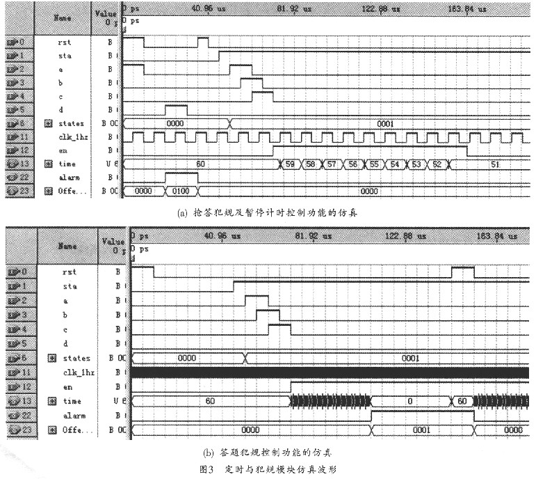
It can be seen from Fig. 3(a) that when rst=1, the answer is invalid, the initial value of the countdown timer is set to 60s; when rst=O, and sta=O, the d group is rushed in advance, the alarm starts to alarm, andoff- Der shows the foul group "0100", indicating that the early foul group is group d. After that, the host presses the rst key to make rst=1. At this time, the alarm stops the alarm and the system enters the initial state. When rs-t=O and sta=1, the group a succeeds, and the timing enable signal en=1. When the rising edge of the clock signal clk_lhz comes, the countdown timer starts counting. When the group a answers the question within the limited time, the host presses the timing enable signal to make en=O, the countdown timer stops, and the alarm is prevented. .
As can be seen from Figure 3(b), when rst=O, sta=1, the a group is successfully answered, but the question is not answered within the time limit. When the 60s countdown time is counted as 0, the alarm starts to alarm, offender Display the foul group as “0001â€, indicating that the timeout foul group is group a; the host presses the reset button to make rst=l, the alarm stops the alarm, the offender displays “0000â€, and the number of the offending group is cleared. The system re-enters the initial state.
2.4 Design of the scoring module The main function of the scoring module is to add points to the successful and correct group, or to reduce the scores of the successful but incorrectly answered groups, and display them through the decoding display circuit. . According to the above functional design requirements, the module needs to add and subtract operations add, sub and system clock clk_lhz as input signals, and the scores of each group are displayed as output signal aa0 [3. . 0], bb0[3. . 0], cc0[3. . o], dd0[3. . 0]; In order to determine which group to add or subtract points, you need to have an input signal for the successful group, you can set it to chose. In order for the system to enter the next round of acknowledgment, the system reset input signal rst should be set. The simulation model of its scoring module is shown in Figure 4. 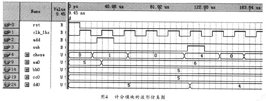
It can be seen from Fig. 4 that when rst=l, the system enters the initial state, and the initial scores of groups a, b, c, and d are all 5. When add=1, when a rising edge of the system clock signal clk_lhz arrives, Add 1 point to the group "0001" that is currently identified by chose. When sub=1, the system clock signal clk_lhz comes to a rising edge, and then subtract 1 point from the "0010" group of the currently identified group.
3 Hardware Verification of Electronic Responder This design uses GW48EDA system produced by Hangzhou Kangxin Electronics Co., Ltd. as the hardware verification system, and selects EP1K30TCl44-3 of Altera Company as the main control chip. The main control chip is a field programmable logic device based on a lookup table structure. Its basic logic unit is a programmable lookup table, which can realize combinational logic operations and can implement sequential logic operations with programmable registers. In design, only the input and output pins in the overall design of the electronic responder should be pin-locked, and then recompiled and downloaded, and the hardware verification of the electronic responder can be performed. Experiments show that this design can realize all the functions of the electronic responder.
4 Conclusion In this paper, the field programmable logic device (FPGA) is used as the design carrier, and the hardware description language (VHDL) is the main expression. The QuartusII development software and the GW48EDA development system are used as the design tools to design a first answer signal identification and An electronic responder that latches, clocks, and scores, and can behave for early warnings and timeouts. The working principle and hardware and software implementation methods of the electronic responder are expounded. The timing simulation and hardware verification of each part of the electronic responder are carried out. The results show that the circuit can achieve its required functions. In addition, because the FPGA chip is small in size, low in power consumption, cheap in price, safe and reliable, the number of answering groups of the responder can be changed with a little modification, and the setting of the answering time and the composition of the results, as well as the maintenance and upgrade are more convenient. It is also easy to make an ASIC chip, so it has a good application prospect.