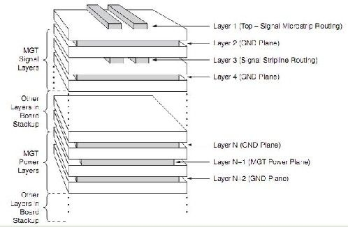
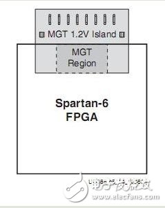
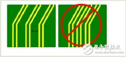
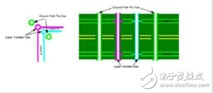
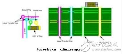
Gigabit-level serial I / O technology has extremely excellent superior performance, but these superior performances require conditions to ensure, that is, excellent signal integrity. For example, one vendor reported that the first time they tried to use a high-speed, gigabit serial design for a specific application, the failure rate was 90%. In order to improve the success rate, we may need to perform simulations and adopt new and more complex bypass circuits. The GTP performance of Spartan-6 FPGA depends on the signal integrity of the PCB. The following factors need to be considered in the PCB design process: the stacked structure of the board, the layout of the components, and the signal routing. Power supply and stack For the GTP transceiver of Spartan-6 FPGA, the stack can be divided into two groups, the power distribution layer and the signal routing layer. The power layer is used to connect GTP's MGTACC, MGTAVCCPLL, MGTAVTTTX and MGTAVTTRX power pins. The laminated structure can refer to the following figure. In the stack above, the ground plane signal transmission line provides a signal return path. At the same time, because there is a shielded plane between the two signal layers, when routing signals, it is possible to disregard the issues that need to be considered when routing adjacent layers, and provide more signal paths. The power plane of the GTP should be closely adjacent to the ground plane to increase the coupling effect. The ground plane can provide shielding for the power plane of the GTP. The shielded power plane comes from the noise interference caused by the signals of the previous or next layer. In fact, from another point of view, when the noise of the power supply appears in the high frequency range, as the frequency increases, it becomes more and more difficult to find a capacitor that can cover this frequency range and achieve a filtering effect until it is impossible to find such a capacitor . As the capacitance value decreases, the related stray inductance and package resistance values ​​do not change accordingly, so the frequency response will not change much. In order to achieve better power distribution at high speed, we need to use the power layer and the ground layer to construct our own capacitors. In order to achieve our goal more effectively, it is usually necessary to use adjacent power and ground layers. The connection between the power pin of the GTP and the power distribution network plays a key role in the working performance of the GTP. PDN and FPGA require a low impedance and low noise connection. The GTP power supply of FPGA can tolerate a maximum noise of 10mVpp. In the range of 10KHz to 80MHz, the power supply can use a small plane. This small power plane should not cover the area of ​​the SelecTIO interface. Capacitor placement In addition to considering the size of the bypass capacitor, another important aspect to consider is the placement of the capacitor. The general rule is that the larger the capacitance, the less stringent the placement requirements. If the capacitance value is small, the capacitor should be as close as possible to the power and ground pins. One method that can be used is to remove unused general-purpose IO traces and vias to make room for bypass capacitors The position of the GTP power supply division area and the position of the GTP filter capacitor can also refer to the following figure. Signal routing GTP signal traces and SelecTIO signal traces should be avoided on adjacent layers, and their respective return paths should also be kept separate, including vias. It is important to maintain a certain distance between differential line pairs and between differential lines and other lines. The general rule is: the distance between adjacent line pairs should be at least 5 times the distance between the two lines in the line pair as shown in the figure below. Gigabit signal differential lines should avoid changing the trace layer as much as possible. If cross-layer transmission is necessary, then special care is required. First, a complete return path must be provided. So we must couple the reference layer of layer A and the reference layer of layer B together. The ideal situation is that both reference layers are strata. In this case, the return path can be achieved by placing another via connecting the two reference planes near the transfer via. The figure below gives a schematic of this technique. If the reference layer is different (one is the ground layer and the other is the power layer), you need to place the ground as close as possible to the via Place a 0.01μF capacitor to connect the two reference layers to reduce the impedance of the return path. As shown below.
The Laptop Stand is completely height adjustable and has six different elevations levels. Aluminum Laptop Cooling Stand is 17 inches wide, which offers plenty of room for your smartphone ,a notebook. Laptop Stand Aluminum Adjustable can find the best viewing angle. The Ergonomic Aluminum Laptop Stand is made of aluminum and comes in black or silver gray, making it an awesome match for Apple`s notebook. Laptop Stands And Risers also features an open-wedge design for better airflow.
Laptop Stand Keyboard is front and back support, turn on the "desktop mode", a large field of view, to bring you a more comfortable viewing angle experience. Laptop Stand Upright six-speed adjustment is just right.
Ergonomic Aluminum Laptop Stand,Ergonomic Portable Laptop Stand For Desk,Adjustable Aluminum Ergonomic Laptop Stand,Ergonomic Aluminum Desk Notebook Holder Shenzhen ChengRong Technology Co.,Ltd. , https://www.laptopstandsupplier.com