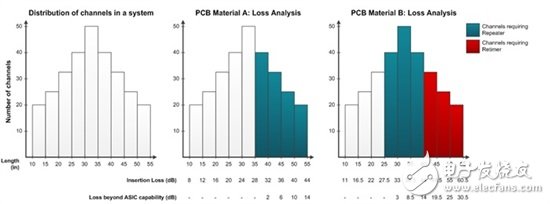
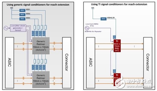
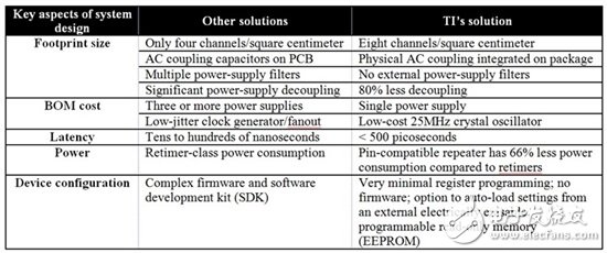
When implementing the transition from 10G to 25G systems for next-generation servers and switches, hardware design engineers must meet these conflicting and contradictory goals: reduce data latency as much as possible, maintain or reduce power consumption, and reduce as much as possible cost. In order to provide data center users with world-class products with competitive cost advantages, fundamentally, you must do more with less. Here are 5 quick tips , which can make you a good balance when designing a 25G system: 1. Determine which link in the system will require signal conditioning; this will depend on the trace length and the printed circuit board (PCB) material. Low-loss materials require less signal conditioning, but they are also more expensive than standard materials. Channels with losses greater than the inherent compensation function of an application specific integrated circuit (ASIC) will require some form of signal conditioning. For example, if your ASIC can achieve a 30dB compensation, you may want to add signal conditioning for channels with a loss of 27dB or more, and the 3dB difference can be used as a safety margin. Figure 1 is an example diagram of a comparison of the channel loss budget analysis between PCB materials A and B. Figure 1: Example distribution of channels in a system, assuming ASIC loss compensation capability: 30dB at 12.9GHz, PCB material A loss: 0.8dB per inch at 12.9GHz, PCB material B loss: 1.1dB per inch at 12.9GHz . 2. For those channels that require signal conditioning, use a small package to achieve design flexibility. The small package provides high channel density and enables you to use retimers or pin-compatible repeaters. 3. Design a power solution that meets the needs of retimers or repeaters. For example, the TPS53513 synchronous buck converter can provide 8A current, which is enough for a group of 6 retimers or repeaters. 4. Determine the SMBus addressing mechanism, which requires individual addressing for each retimer/repeater device on the circuit board. You can use one of 16 unique SMBus addresses to configure each device pin. If there are more than 16 devices on a board, consider using an I 2 C expander such as the TCA/PCA series I 2 C/SMBus switch to divide the SMBus into multiple buses. 5. Place a single low-cost 25MHz (±100ppm) 2.5V single-ended clock on the circuit board to support up to 20 retimer devices. Since it is not used to recover data, this clock does not have any jitter requirements. This retimer will accept the clock time, buffer it, and copy it on an output pin for easy connection to the next retimer. There is no need to use multiple crystals or fan-out buffers. If you finally decide to use a repeater instead of a retimer, then you can choose not to assemble this component to reduce costs. In order to make the above techniques easier to implement, TI has introduced the industry's first pin-compatible repeater (DS280BR810) and retimer (DS250DF810) solution product portfolio to implement 25G backplane and front port applications. And how do these help achieve a balance between power consumption, performance and price? All this is related to design simplicity and flexibility. TI’s pin-compatible repeater and retimer solutions enable you to choose a solution that meets your performance goals while minimizing latency and lowering bill of materials (BOM) costs. Hardware engineers know that the cost, size, and complexity of surrounding components are as important as the repeater or retimer itself. Consider the circuit board design example in Figure 2. Figure 2: Graphical representation of the simplicity and cost savings of a TI solution (on the right) compared to a common solution (on the left) Table 1: Comparison between TI’s 25G signal conditioning solutions and other solutions The pin-compatible properties of TI’s 25G DS280BR810 repeater and DS250DF810 retimer solutions enable you to generate a schematic circuit diagram to evaluate these two options to achieve cost, power consumption, and performance optimization for the final product. Signal integrity engineers can start testing with a repeater solution, which provides lower cost and power consumption. If the jitter and crosstalk in the system require higher performance, they can be upgraded to a pin compatible retimer solution. Small objects really have a big effect. Imagine a common data center with 20,000 servers. Using a repeater instead of a retimer can save a server network interface card (NIC) about 1W of power consumption, and the total annual electricity savings are more than 21,000 US dollars (0.12 US dollars per kilowatt-hour), which is not Including the cooling costs saved. If you reduce the BOM component cost by $5, you can save an additional $100,000. Finally, the difference between a 50ns delay and a 500ps delay is that while satisfying the entire data center service request, 8 hours of time will be "wasted" every day (assuming that there are 2000 requests per second, the total usage time of each server per day is 4 hours). By using these techniques, you should be able to design a circuit board that balances cost, power consumption, and performance.
UCOAX specializes in custom drawing, flattening, stranding and insulating, cutting and stripping of fine wire and cable .0009" (AWG #48) and larger.
UL iQ for appliance wiring materials
Single-Conductor, Themoplastic Insulation
1007 1015 1061 1185 1126 1227 1330 etc.
Multiple-Conductor, Thermoset Insulation
2464 2468 2725 2835 2990 20276 20379 21100 21118
Single-Conductor, Thermoset Insulation
3173 3265 3266 3271 3272 3302 3346 3347 3363 3383 3385 3386 3619
For more details, please feel free to contact us, thank you.
Ul Wiring Material,Ul Wiring Material Components,Electrical Wire Materials,Wiring Material UCOAX , https://www.ucoax.com