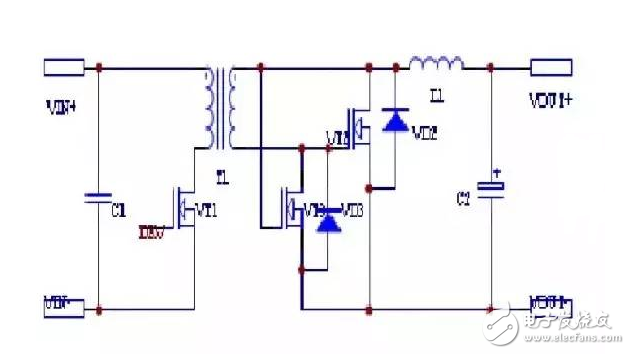
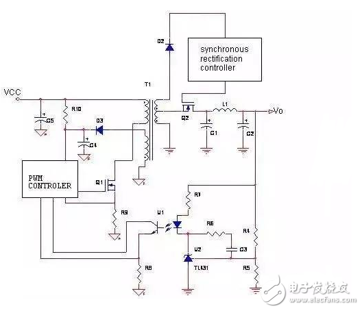
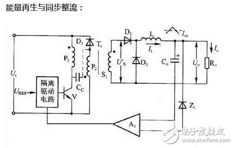
It can be seen from the synchronous rectification schematic diagram that the driving voltage of the rectifier VT3 and the freewheeling tube VT2 is taken out from the secondary winding of the transformer, and is applied between the gate G and the drain D of the MOS transistor, if the MOS transistor is in a separate circuit. Such an application cannot be fully turned on and the loss is large, but it is a feasible simplification scheme for synchronous rectification. Since the two tubes are in a state of trivial switching, one tube is open and the other is closed, so we only briefly analyze the opening of the inductor current continuously. We know that the MOS tube has anti-parallel diodes in the body, so that the inductor current is continuously applied. The diodes connected in parallel before the MOS tube is turned on are turned on, and the levels of the source S and the drain D are aligned with respect to the gate. The voltage applied between the GD is equivalent to the voltage applied between the GS, so that the secondary winding of the transformer is the same When the terminal is positive, the gate leakage voltage of the rectifier VT3 is positive, and the zero voltage of the rectifier is turned on. When the secondary winding of the transformer is negative, the freewheeling tube VT2 is turned on, and the filter inductor continues to flow. The gate voltage must be synchronized with the phase of the rectified voltage to complete the rectification function, so it is called synchronous rectification. Synchronous rectification is a new technology that uses a dedicated power MOSFET with very low on-resistance to replace the rectifier diode to reduce rectification losses. It can greatly improve the efficiency of the DC/DC converter and there is no dead zone voltage caused by the Schottky barrier voltage. Power MOSFETs are voltage-controlled devices that have a linear relationship in volt-ampere characteristics during turn-on. When using a power MOSFET as a rectifier, it is required that the gate voltage must be synchronized with the phase of the rectified voltage to complete the rectification function, so it is called synchronous rectification. The development of electronic technology has made the operating voltage of the circuit lower and lower, and the current is getting larger and larger. Low-voltage operation helps to reduce the overall power consumption of the circuit, but it also poses new challenges for power supply design. The loss of the switching power supply is mainly composed of three parts: the loss of the power switch tube, the loss of the high frequency transformer, and the loss of the rectifier at the output end. In the case of low voltage and high current output, the conduction voltage drop of the rectifier diode is high, and the loss of the rectifier at the output end is particularly prominent. Fast recovery diode (FRD) or ultra-fast recovery diode (SRD) can reach 1.0-1.2V, even with a low-dropout Schottky diode (SBD), it will produce a voltage drop of about 0.6V, which leads to increased rectification losses. Large, power efficiency is reduced. For example, some CPUs use a 3.3V or even 1.8V or 1.5V supply voltage, which can consume up to tens of amps. At this point, the rectification loss of the ultrafast recovery diode is close to or even exceeds 50% of the power output. Even with Schottky diodes, the loss on the rectifier will reach (18% to 40%) PO, accounting for more than 60% of the total power loss. Therefore, the traditional diode rectification circuit can not meet the needs of achieving high efficiency and small volume of low-voltage, high-current switching power supply, and becomes a bottleneck restricting the efficiency of the DC/DC converter. Both rectifiers can be viewed as a gate through which current flows through the gate for load. The traditional rectification technology is similar to a door that must be pushed through someone's push. Therefore, every time the current passes through the door, it has to work hard, and it is sweating, and the loss is naturally quite a lot. The synchronous rectification technology is similar to the induction door of the higher-end venue we passed: it seems to be closed, but when you go to it and need to pass it, it will open itself, and you don’t have to push it yourself. So naturally there is no loss. Through the above analogy, we can know that the synchronous rectification technology greatly reduces the rectification loss at the output end of the switching power supply, thereby improving the conversion efficiency and reducing the heating of the power supply itself. When the switching transistor V is turned on, the electrical energy received by the transformer is transmitted to the output terminal in addition to the magnetizing current. During the flyback of the tube V, the guiding diode D2 is reverse biased so that there is no loop of clamping or energy bleed. The magnetizing energy will generate a large back pressure between the collector and the emitter of the switching tube. In order to prevent the generation of high back pressure, an "energy regeneration winding" P2 is provided, and the stored energy is fed back to the direct current power source Ui by the winding P2 through the diode D1. As long as the relationship of Wp1=Wp2 is satisfied, and when Up1=Ui when D1 flows current, the collector-emitter voltage on the switching transistor V is 2Ui. In order to avoid excessive leakage inductance between the P1 and P2 windings, and thus excessive voltage on the collector of the switching transistor, a method in which the primary winding P1 and the energy regenerative winding P2 are wound in a double line is generally employed. In this configuration, it is important that the diode D1 is connected to the position of the energy regenerative winding as shown. The reason is that the internal stray capacitance Cc caused by the double-wire winding is a parasitic capacitance between the collector of the switching transistor V and the connection point of the windings P2 and D1. According to the connection method in the figure, there is an advantage. For example, when the switching tube V is turned on, since the diode D1 is reversed and the collector is separated, no current flows into the capacitor Cc when V is instantaneously turned on (note that) The non-identical ends of the windings P1 and P2 become negative at the same time, and the voltage across Cc does not change). However, during the flyback period, Cc provides the clamping action of the switching transistor V. Any overvoltage trend will cause the Cc to flow current, and after D1, it is fed back to the power line. If the parasitic capacitance is not large enough, only the P1 and P2 windings are magnetically coupled. When the clamp voltage is overvalued, an external capacitor can often be added at the % position to improve its clamping effect. However, if the capacitance value is too large, there will be a voltage component of the input voltage å½ ripple frequency modulation on the output voltage line, so the value of the additional capacitor Cc should be carefully selected. When the switching transistor V is turned on, the input voltage Ui is applied to (Lp+LLT), and since D2 reverse bias prevents charging of C2, Uc2 ≈0. When the switching transistor V is turned off, the collector voltage Uc of V rises rapidly due to the flyback, but since the ç € is turned on by the positive bias at this time, the V current is shunted by C2 and R1, and the Uc voltage gradually rises, that is, The UD1 voltage is also gradually rising and clamped to a value of 2Ui. This eliminates the top of the spike voltage at which Uc rises, as indicated by the dashed pulse peak. For the remainder of a cycle, as the R1 discharge current decreases, the voltage drop across C2 will return to its original value. Excessive flyback energy is consumed on R1. This clamp voltage is self-tracking, during steady state operation, because the voltage on C2 is automatically adjusted until all excess flyback power is consumed on R1. If in all other cases, a constant clamp voltage is maintained, the increase in the clamp voltage can be suppressed by reducing the value of the R1 value or the leakage inductance Lyp. The clamp voltage cannot be designed too low because the flyback voltage has a useful side. In the case of flyback, it provides an additional forced voltage value to drive electrical energy into the secondary inductor. The flyback current of the transformer secondary is rapidly increased. The transmission efficiency of the transformer is improved, and the loss on the resistor R) is also reduced. This makes sense for low voltage and high current output. (1) The circuit is simple and uses less devices. (2) When there is no filter circuit, the DC component of the rectified voltage is small, Vo=0.45V2 (3) The ripple of the rectified voltage is large. (4) The utilization rate of the transformer is low. (1) The rectifier device used is twice as large as the half-wave rectification. (2) The rectified voltage ripple is small, which is less than half of the half-wave rectification. The output voltage Vo = 0.9V2 when there is no filter circuit. (3) The utilization rate of the transformer is higher than that of the half-wave rectification. (4) The secondary winding of the transformer needs a center tap. (5) The rectifying device is subjected to a high reverse voltage. (1) The rectifier device used is twice as large as that of full-wave rectification. (2) The rectified voltage ripple is the same as the full-wave rectification. (3) The reverse voltage that each device is subjected to is the peak value of the power supply voltage, that is. (4) The utilization rate of the transformer is higher than that of the full-wave rectifier circuit. Multipole Ferrite Ring Magnet y25, Multipole Ring Ferrite Magnet HU NAN YUBANG MAGNETIC MATERIAL CO.,LTD , https://www.ybmagnet.com


What does synchronous rectification in current mean? What is the significance of synchronous rectification? Half wave full wave bridge rectifier circuit
Synchronous rectification works: