Design of Radar Antenna Power Failure Detection Circuit Introduction With the widespread use of phased array antennas in radar, fault detection of antenna power supplies has become increasingly important. The power supply scale of phased array antennas is often proportional to the number of transceiver (T / R) components. When there are hundreds of R components, the power supply system is relatively large, and the power failure detection is more complicated. The power failure will directly cause the T / R component to work abnormally. Therefore, it is very important to design a perfect power failure detection circuit. Carry out monitoring, find faults in time, locate faults to LRU, and guide maintenance personnel to perform replacement parts repair. Circuit Design Signal Conditioning Circuit Signal conditioning circuit mainly processes the input power detection signal by filtering, voltage division and impedance matching. The purpose of filtering is to filter out high-frequency glitches in the detection signal. It can be seen from the experiment that there are often interference glitches with large amplitude in the antenna power signal. If not filtered, it may cause damage to the device or affect the detection accuracy. The purpose of voltage division is to change the amplitude of the detection signal to meet the input requirements of the subsequent A / D converter. The key to the design is to ensure that the amplitude of the signal does not exceed the input requirements of the A / D, and to maximize the signal Resolution. The impedance matching circuit is an emitter follower, the purpose is to perform impedance matching before and after, to improve the accuracy of detection. Figure 2 is the conditioning circuit for the 12V detection voltage. Figure 2 12V detection voltage conditioning circuit Capacitor C1 filters high-frequency glitches, generally 0.01μF, precision resistors R1 and R2 form a voltage divider circuit, in order to reduce the impact on the power supply, the resistance value should be in the order of 1000 ohms, the specific value should refer to the normal judgment of 12V Range (10.3 ~ 14V) and A / D full scale range (0 ~ 2.55V), after calculation and trade-off, R1 takes 46.4KΩ, R2 takes 10KΩ, and the undervoltage and overvoltage thresholds of 12V voltage can be calculated respectively for: Figure 3 MUX circuit The MUX circuit is shown in Figure 3. The main function is to select the 35 voltages to be measured to ensure that only one voltage enters the analog-to-digital conversion circuit of the subsequent stage for data conversion at a certain moment. The MUX circuit is composed of two stages. The pre-stage is composed of five multiplexers of eight choices. The 35 measured voltages are connected to these MUXs after conditioning. Only two wiring diagrams are drawn in the figure, and the rest The three blocks are basically the same, and the rear stage is composed of a multiplexer, which further selects the five voltages output by the front stage. In the figure, the signals MUX1 and MUX2 select the front-end chip, the signals DD0, DD1, and DD2 select the front-end channel, and the signals DD5, DD6, and DD7 select the back-end channel. These signals are generated by CPLD and are designed specifically. Please refer to Section 2.5 Design of CPLD Internal Logic Circuit. Figure 4 Analog-to-digital conversion circuit Figure 4 is an A / D conversion circuit. The main function is to perform data conversion on the input measured voltage, and the conversion result is sent to the microcontroller. The A / D conversion device uses AD670 of ADI Company, eight-bit resolution, 10μs conversion speed, programmable unipolar or bipolar input, unipolar full-scale input range is 0 ~ 2.55V, bipolar is -1.28 ~ + 1.27V, the signal ADRDY in the figure is the A / D conversion completion signal, connected to the I / O pin of the microcontroller, when ADRDY is low, it means that the data conversion is completed, and the A / D is judged by querying the status of the signal in the program Whether the conversion is complete. The signals ADCE, ADCS, and ADRW are the chip enable, chip select, and read / write control signals of A / D, respectively. ADCE and ADCS are low and effective, and they are connected to the address lines P20 and P21 of the single-chip microcomputer, respectively. Operations, that is, write control commands, such as unipolar or bipolar operations, etc. When ADRW is high, the A / D is read and the conversion result is read out. This signal is generated in the CPLD. Figure 5 SCM and peripheral circuits Figure 5 is a single-chip microcomputer and peripheral circuits. The single-chip microcomputer uses AT89C55 of ATMEL company. It has 20K bytes of program memory inside. It is the control core of the entire fault detection circuit. It runs the program to control the detection circuit to perform voltage detection and conduct the detection results. Initial processing, generating unit-level fault table, send to higher level for comprehensive processing. The integrated circuit D2 (MAX813) is a watchdog. Its main function is to monitor the running status of the program of the single-chip computer. If the program runs for more than 1.6 seconds, the watchdog generates a reset signal to reset the single-chip computer, so that the program enters the normal steps again. The integrated circuit D3 (MAX485) is an RS-485 serial communication interface, which realizes the mutual conversion between TTL level and RS-485 level, and is the communication interface between the detection circuit and the superior unit. Diode V2 is a fault indicator. When a power failure is detected, the indicator is lit. Figure 6 CPLD logic circuit Conclusion At present, the antenna power failure detection circuit has been applied to a radar. With the design of the radar system, it has entered the mass production stage. Practice has proved that the detection circuit is stable and reliable, and can accurately and real-time monitor the antenna power system for fault detection. Rate ≥98%, fault isolation rate ≥95%, false alarm rate ≤3%, meet the design requirements. Load Pins,Load Pin Load Cell,Oem Load Cells,Strainsert Load Pin Xiaogan Yueneng Electronic Technology Co., Ltd. , https://www.xgsensor.com
The power failure detection circuit is composed of hardware and software. The hardware block diagram is shown in Figure 1. The signal conditioning circuit filters, divides the voltage and impedance of the 35 input power detection signals, and then selects the analog-to-digital converter (A / D) through the multiplexer (MUX), converts it into a digital quantity, and reads it into the single chip The digital quantity is compared with the specified upper and lower limits to determine whether the voltage is correct. Finally, a unit-level fault table is generated and transmitted to the superior through the RS-485 interface for further processing. 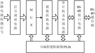
Figure 1 Block diagram of hardware 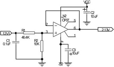
Undervoltage threshold: 1.83V
Overvoltage threshold: 2.48V
That is, the normal range of the input 12V voltage after voltage division should be in the range of 1.83 ~ 2.48V, otherwise it is judged as a fault.
Multiplexing circuit 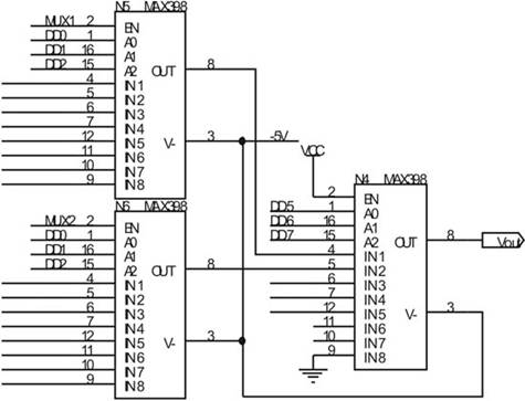
Analog-to-digital conversion circuit 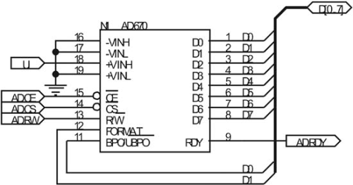
SCM and peripheral circuits 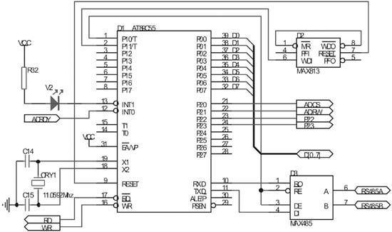
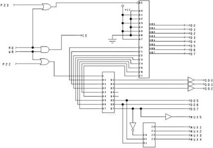
CPLD logic circuit Figure 6 is the internal logic circuit of CPLD. CPLD uses the ispLSI1016E of LATTICE company. The logic design uses the schematic input method. The main function is to select the MUX channel, control the A / D converter, and generate the self-test code. Wait. There are three main devices in the picture: data bidirectional switch, data latch, and decoder. When the OE of the data bidirectional switch is low, the data A0 ~ A7 are transferred to the data lines D0 ~ D7 of the MCU. When the data is normal, it is the self-check code AAH. When OE is high, the MCU data is transferred to the latch inside the CPLD. Used to select multiple analog switches. Port address decoding uses the RD, WR, P22, P23 pins of the single-chip microcomputer, and also uses the P20 and P21 pins of the single-chip microcomputer. They are connected to the A / D converter CS and CE respectively. The specific addresses are defined as follows:
CPLD self-test address: 0x0700
Channel selection data latch address: 0x0b00
A / D converter write address: 0x0c00
A / D converter read address: 0x0e00
The signals MUX1 ~ MUX5 are the chip selection signals of the previous stage of the MUX circuit, and the high level is effective; DD0 ~ DD2 are the channel selection signals of the previous stage of the MUX circuit, and the value range is 0 ~ 34, corresponding to 1 ~ 35 of the analog channel; DD7 is the channel selection signal of the latter stage of the MUX circuit, with a value range of 0 to 4, respectively corresponding to the output signals of the five MUX of the previous stage. The generation process of these signals is: the single-chip microcomputer sends the channel selection data and chip selection data to the latch through the data lines D0 ~ D7, generates the channel selection signals DD0 ~ DD2 and DD5 ~ DD7, and then decodes part of the data to generate the MUX Chip selection signals MUX1 ~ MUX5.