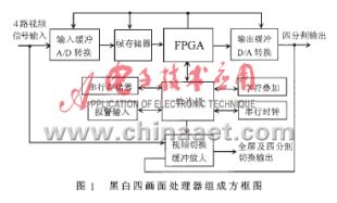
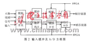
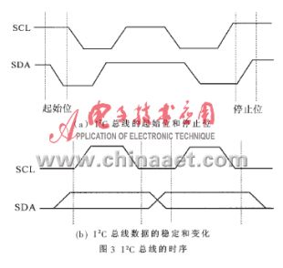
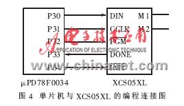
In recent years, with the wide application of video surveillance systems in various fields, the application of multi-picture processors, which is one of the components of video surveillance systems, has become more and more popular. If you use a nine-screen processor, you can monitor 9 targets simultaneously on a single monitor, and you can simultaneously record 9 channels of video signals in real time with just one recorder. At present, the multi-picture processor has six types of black and white/color four, nine, sixteen picture processors. In general, in addition to the screen splitting function, the multi-picture processor must also have video signal switching and alarm functions. The video signal power conversion function refers to the multi-picture processor having one video output which is the sequential switching of the input video signal or the picture division signal, and the switching time is adjustable; the alarm function means that the multi-picture processor can input and output the alarm signal, and the alarm time Alarm information is superimposed on the corresponding screen, and the alarm information is stored for later reference. The design of the multi-picture processor can use a dedicated DSP chip, so although the speed requirement is met, the development cycle is long, and the debugging, modification and upgrading of the product are difficult and the cost is high. Because FPGA (ie, field programmable gate array) devices have high integration, small size, low power consumption, flexible design and low price, and have a fast and efficient development platform, which can accelerate the development cycle and other advantages, so the current multi-screen processor The design basically uses FPGA as the video signal processing device among them. Since the function of the FPGA is determined by its internal programming data, one of the loading methods of the programming data is implemented by the single chip microcomputer after power-on, so the multi-picture processor contains the single chip microcomputer. On the one hand, the microcontroller needs to write the programming data required by the FPGA into the FPGA after power-on. On the other hand, the switching of the video signal, the character superposition and the processing of the alarm information are also completed by the single chip microcomputer. The following describes the design method of black and white four-picture processor based on FPGA device and single chip microcomputer. This article refers to the address: http:// 1 Black and white four-picture processor composition and main functions 1.1 Composition of black and white four-picture processor The block diagram of the black and white four-picture processor is shown in Figure 1. As can be seen from FIG. 1, the multi-picture processor is composed of an FPGA device and a single chip microcomputer, and is supplemented by auxiliary chips such as A/D, D/A, frame memory, serial memory, serial clock, and character overlay. 1.2 main functions of black and white four-picture processor The main functions of the four-picture processor are as follows: · The video format is CCIR mode, that is, the field frequency of the video signal is 50 Hz; ·Duplex operation (playback can be performed while recording), menu setting; · The full-screen display pixel is 1024 × 512, 256 gray levels; · 4 channels of CVBS input and 1 channel of video input; · 1 channel full screen and 4 division switching output, 1 channel video output (fixed four division); · The switching time is adjustable from 1 to 255s. · The date and time can be superimposed on the screen, and the position can be adjusted; · There is alarm input and output function, the alarm reset time can be adjusted from 1 to 300s; · There is a video signal loss alarm function, and there is a text display on the corresponding screen when the alarm occurs. 2 The structure and working principle of each part of the circuit 2.1 Input buffering and A/D conversion The main function of this part of the circuit is to convert the input analog video signal into a digital video signal for processing by the FPGA device. The block diagram is shown in Figure 2. After 4 channels of video signals pass through the analog multi-channel selector controlled by FPGA, 2 channels of video signals are output, which are buffered and amplified and sent to the analog switch controlled by FPGA; then output to A/D, 2 channels of video signals need 2 pieces A/D chip. The A/D chip selects the TLC5510, which is a CMOS analog-to-digital converter with 8-bit resolution and 20MSPS (20 megasample points per second). Under the control of the FPGA, the TLC5510 converts the input analog video signal into a digital video error and sends it to the frame memory. 2.2 Frame Memory The frame memory is selected by AVERLOGIC's AL422, which requires a total of 2 pieces. AL422 is a FIFO (First In First Out) DRAM with 384KB×8Bits. It supports VGA, CCIR, NTSC, PAL and HDTV resolutions with independent read/write operations and output enable control. The storage time is 15ns. High-speed asynchronous serial access for operation from a 5V or 3.3V supply voltage in a standard 28-pin SOP package. 2.3 FPGA device FPGA is the core of this design and has a different structure than traditional logic circuits and gate arrays. The FPGA uses a small lookup table (16 × 1 RAM) to implement the combinational logic. Each lookup table is connected to the input of a D flip-flop, which in turn drives other logic or drives I/O. These modules are interconnected or connected to I/O modules using metal wires. The FPGA realizes its logic by loading programming data into the internal static memory cell by loading the programming data into the internal static memory cell. The value stored in the memory cell determines the function of the FPGA implementation; this structure of the FPGA allows an infinite number of times. Reprogramming. It can be seen that the debugging and upgrading of the product designed by FPGA is easy and has great flexibility. At present, there are many types of FPGAs, and the Spartan series XCS05XL is used in this design. The chip is a low-cost, high-performance FPGA from Xilinx. Its main features are as follows: · The number of system gates has reached 5,000, the number of Logic cells has reached 238, and the system resources are abundant; · With on-chip programmable distributed RAM, up to 3200bit of programmable RAM; Distributed arithmetic logic unit that supports distributed DSP operations; Flexible flexible high-speed clock network, internal tri-state bus; operating voltage is 3.3V. For more information on the XCS05XL, please refer to reference [1]. The programming data of the FPGA is stored in the FLASH ROM of the microcontroller. After each power-on, the MCU loads the programming data into the XCS05XL. The programming mode selects the slave mode, so its 22-pin (M1) and 24-pin (M0) are left floating. After the programming data is loaded, the logic function of the XCS05XL is determined; the XCS05XL controls the input and A/D conversion of the video signal, and internally compresses each video signal to 1/2 of the original video signal, and gives each one under the control of the single-chip microcomputer. The road superimposes the time, date, and channel digital character information, and then combines the compressed four video signals into one complete digital video signal, and outputs it to D/A to form a four-divided output. 2.4 D / A conversion and output buffer amplification The D/A conversion circuit converts the digital video signal output by the FPGA into an analog video signal, and then outputs the buffer to the monitor, and the D/A chip selects the HI1171. The chip is a high-speed D/A converter with a resolution of 8 bits and a frequency of 40MHz. The maximum integral and differential linearity errors are 1.3LSB and 0.25LSB respectively. The minimum settling time is only 5ns, working at a single 5V. The power consumption is only 80mW. The output buffer amplification consists of discrete components. 2.5 single chip microcomputer The single chip selects the μPD78F0034 of NEC Corporation of Japan. The main features of the chip are: · The instruction cycle when the clock is 8.38MHz is 0.24μs; · ROM is 32KB FLASH, RAM is 1024bytes; · Addressable space is 64KB, 5 external interrupts, 15 internal interrupts; 39 CMOS I/O, 8 COMS INPUT, 4 N-CH open-drain I/Os; · 1 16-bit timer/counter, 2 8-bit timer/counters; · 1 clock timer, 1 watchdog timer, 1 UART port; · Support I2C bus, with clock signal and buzzer output function; · External data bus 8 bits, internal register is 16 bits; · 8-bit unsigned multiply instruction, 16-bit division instruction; ·The operating voltage range is 1.8V~5.5V, and there is STOP/HALT working mode. It can be seen that the performance of the chip is better than the current popular MCS-51 series, and its 8-bit unsigned multiply instruction and 16-bit division instruction bring great convenience to software programming. In addition, since the chip itself has a watchdog timer, the system can be operated stably and reliably without the need for an external watchdog circuit. 2.6 memory The memory chip uses a serial EEPROM chip X24C16. The chip is a 2KB write-protected I2C bus data memory. When WP=1, it can only read and cannot write data. It uses a serial data line (SDA) and a serial clock line (SCL) for data transfer between the master and slave devices. The data transmission rate on the I2C bus can reach 100Mbps, and in the fast mode up to 400Mbps. In the I2C bus transmission, the start and stop conditions are defined as follows: when SCL is high, SDA changes from high to low; when SCL is high, SDA changes from low to high (see Figure 3(a) Shown). Both SDA and SCL are bidirectional transmission lines. The data on the SDA line must be stable during the period when the clock is high. Only when the clock signal on the SCL line is low, the state on the data line can be changed (see Figure 3(b). Shown). Each byte output to the SDA line must be 8 bits, and the bytes transferred each time are unrestricted, and each byte must have an acknowledge bit. In this design, the 5th pin (SDA) and the 6th pin (SCL) of the X24C16 are connected to P3.6 and P3.7 of the MCU respectively. 2.7 Clock and Character Superposition Circuit The clock chip selects the serial clock DS1302. The chip is a high-performance, low-power, real-time clock chip with RAM, which has the following main features; · Real-time clock, which can count seconds, minutes, hours, days, weeks, months, years, and has leap year compensation function until 2100 years; · 31B NV RAM for data temporary storage, simple three-wire interface, TTL compatible; • Continuous multi-byte data transfer for clock or RAM data read/write; 8-pin DIP or 8-pin SOIC package for surface mount; · Operating voltage is 2 ~ 5.5V, temperature is -40 ° C ~ 85 ° C. The character superposition circuit is composed of NEC company μPD6453. The chip can display 12 lines on the screen, 24 characters per line, and each character is 12×18 dot matrix. The size and flashing frequency of the characters can be adjusted as needed. The background color of the screen, the edge color of the characters, and the color of the characters themselves can also be modified. In addition to curing the characters of 191 Japanese characters, English letters and numbers, the chip also solidifies 49 Chinese characters (such as year, month, day, and hour); in addition, the chip provides 16 characters of RAM space. Allow users to fill in custom characters. Since the picture processor does not need to superimpose too many different characters, the design does not add a Chinese character font, which saves cost and space of the circuit board, and simplifies the circuit structure. The line, field sync, and clock signals required for the μPD6453 are provided by the FPGA. The MCU sends a series of commands (including the characters or characters to be displayed, the size of the characters, the spacing of the characters, and the attributes of the characters) to the μPD6453 through serial data transmission. After receiving the command, the μPD6453 sends the information to be displayed or Chinese characters. To the FPGA. 2.8 video signal switching circuit This circuit consists of the MAX440. The MAX440 is a high-speed multi-channel video selector switch with a wideband video amplifier that can input eight video signals and output one video signal. Under the control of the single-chip microcomputer, the output can be connected to any of the eight video inputs. The main features of the chip are as follows: · The bandwidth is 110MHz; the differential gain is 0.04%, and the differential phase is 0.03 degrees; · Switching time is 15ns, and the conversion rate is 370V/μs; • The input capacitance is 4pF when on/off, eliminating the need for an external compensation component. 2.9 Reception and processing of alarm signals Directly completed by the microcontroller, without going through the FPGA. When an alarm occurs, the MCU receives the alarm message, issues a command to make the buzzer sound an alarm, and notifies the FPGA and μPD6453 that the corresponding screen flashes and the word “alarm†appears. 3 FPGA device XCS05XL programming implementation principle The so-called programming is to use the microcontroller μPD78F0034 to load the pre-designed data into the XCS05XL in some way to determine the function of the CLB and IOB inside the XCS05XL and the connection mode of the routing channel. The data writing is only done during the programming process. During normal operation, the memory cells are only used to provide fixed control signals, and the programming memory cells are distributed in an array in the XCS05XL. Each CLB has hundreds of programming data bits, and each programming data bit defines the state of a static memory cell that can control a logic function lookup table bit, a data selector input, or an interconnect switch transistor. The Xilinx development system converts the logic design into a network table file that automatically partitions, sets, and routes the logic, generates programming data in PROM format, and stores the data in the PROM. The XCS05XL has three programming modes: slave mode, main string mode, and fast mode. Before programming begins, the chip automatically detects the M1 and M2 pins to determine the programming mode. After programming, these pins are useless. When the M1 and M2 pins are high, the slave mode is selected, which is also the most commonly used programming mode. In fact, the M1 and M2 feet can be left floating at this time. If the main string mode is to be selected, the M1 and M2 pins must be connected or grounded through a 1k°C pull-down resistor. Figure 4 shows a schematic diagram of the μPD78F0034 microcontroller loading and editing data for the FPGA device XCSO5XL. The programming mode of XCS05XL is selected from the serial mode, so its M1 and M2 pins are floating (ie, equivalent to high level). The edit data of the XCS05XL is stored in the FLASH ROM of the MCU. After the power-on reset, the MCU serially transfers the data to the XCSO5XL through the P30 pin. The programming clock (CCLK) signal required by the XCS05XL is generated by the microcontroller. On each rising edge of CCLK, the XCS05XL receives input data via the DIN pin. 4 Several issues to be aware of when designing hardware and software (1) Problems to be aware of when using frame memory AL422 Since the frame memory AL422 is a FIFO DRAM, it is necessary to ensure that the WCK and RCK signals are always present and the frequency of the signal is not lower than 1 MHz, since the higher frequency of WCK and RCK will be used as the refresh clock signal of the DRAM. · On the rising edge of the /422S/RRST signal, the /RE signal cannot be low, which should be noted when determining the programming data of the FPGA (since the /RRST and /RE signals are provided by the FPGA); ·AL422 can work under 5V or 3.3V power supply voltage. When using 5V power supply, its DEC pin (Pin19) must be connected with 2.2μF decoupling capacitor; when using 3.3V power supply, DEC pin (Pin19) can be directly connected with 3.3. V is connected and bypassed to ground with a 0.1μF capacitor; the capacitors are all tantalum capacitors. Since 3.3V is used, the power consumption of the device is low and the noise is small, so the 3.3V power supply is used to power the AL422 in this design. (2) In order to avoid crosstalk between video signals, various analog video signals are separated by thick ground lines, and the video lines are wide enough. The above describes the design of the black and white four-picture processor. In order to save board space and make the product small and compact, all components and IC chips are packaged in a chip package. Due to space limitations, this article does not discuss the design of multi-picture processor software. As for the design of the 9-picture and 16-picture processors, the design idea and composition block diagram are similar to the 4-picture processor, except that A/D, AL422 and FPGA are added, and the software programming is also complicated. Smart Terminal,Cba Smart Terminal,Smart Payment Terminal,Pos Smart Terminal Guangzhou Winson Information Technology Co., Ltd. , https://www.winsonintelligent.com