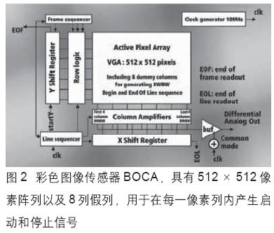
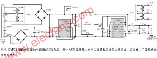
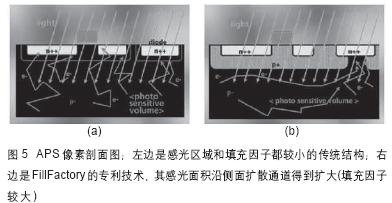
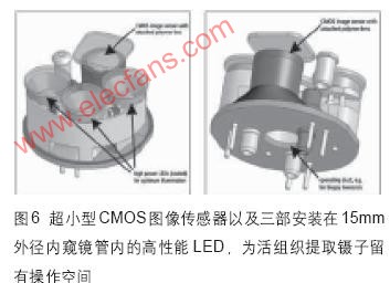
Medical technology has always been one of the important application areas of CCD (Charge Coupled Device) image sensors. Now, CMOS sensors have entered a period of rapid development. The reason, first of all, CMOS image quality is comparable to CCS images. Second, CMOS sensors have a large price advantage in terms of standard semiconductor manufacturing processes. Third, the infinite potential of CMOS sensors in circuit integration can reduce the number of input and output interfaces. Based on a special CMOS image sensor that can be discarded after one use, a new type of low cost colonoscope has been developed. This colonoscopy eliminates the need for costly sterilization of colonic diagnostic equipment, thus avoiding the possibility of any infection. This device is small in size and can perform almost painless inspections. Because CCD image sensor has many advantages such as high resolution, low noise, small dark current and large sensitivity range, medical image acquisition has always been an important application field of such image sensors. On the other hand, the development of CMOS sensors in recent years, especially in the use of small-sized pixels to achieve high resolution and reduce noise and dark current levels, has made CMOS sensors an increasingly widespread application. Cost equipment. From the various fields of X-ray image acquisition and endoscopy, to the "camera in the pill" with its own characteristics, the application field of CMOS sensors can be described as comprehensive. CMOS technology features The natural advantage of complementary metal oxide semiconductor (CMOS) technology is that it can incorporate CMOS logic on the sensor chip to integrate image acquisition with control, conversion and sensing functions [1]. Its high integration density makes it possible to implement small single-chip systems. The integration of more system functions to develop autonomous optoelectronic sensor systems is currently only limited by economic factors such as return on investment, market capacity and development costs. Single-chip solutions stand out in their class of solutions due to the advantages of fewer external components and interconnects, which are of great importance for endoscopes with small diameters. High integration is synonymous with low cost, and CMOS image sensors are therefore favored by various types of endoscopic applications. Due to the low power consumption, CMOS image sensors are also suitable for the manufacture of autonomous small cameras that can be mounted in pill-sized boxes and wirelessly transmit data to the receiving station. In addition, CMOS technology can also be used in the production of radiation protection products, which are generally more resistant to ionizing radiation (ionizingradiaTIon) than CMOS image sensors [2]. A slight improvement in CMOS technology with thicker epitaxial layers or back-lighting can improve the near-infrared (NIR) sensitivity of the sensor, leading to new medical image processing applications (such as near-infrared-based tomography [3] ). Cost-effective splicing technology enables the production of large (up to wafer level) CMOS image sensors using 8-inch wafers and 12-inch wafers in the future. Small image sensor for endoscope In order to create a new type of disposable endoscope (Fig. 1), STMMedizintechnik [4] in Kissing, Germany, needed a low-cost image sensor that could only be produced using CMOS technology. To this end, Cypress/FillFactory, an expert in the field of CMOS image sensors, has successfully developed a small color image sensor BOCA using 0.35 μm CMOS processing technology. The BOCA has a 9mm2 sensor area and is composed of 512 x 512 square pixels each 6 μm long. This sensor's 58% fill factor is a powerful guarantee for high sensitivity (Figure 2). The sensor spectral response ranges from 400 to 1000 nanometers. The pixel frequency is 10MHz and the output is 20fps at 50ms integration time. The shutter selection triggers a rolling shutter (triggered rolling shutter). At full speed of 20 fps, this image sensor consumes approximately 36 mW. Clock generators and fixed pattern noise (FPN) corrections are integrated on the chip. Image sensor prototypes are used to ensure that the product conforms to the target specifications, from which negligible deviations in the manufacturing process can be seen. The noise measurement is 63eˉ, which is within the acceptable range; the signal-to-noise ratio is 522:1 and the dynamic range is 54dB. The dark current at room temperature was 78 pA/cm 2 ; the dark current at body temperature (37 ° C) was 188 pA/cm 2 . Fill factor and quantum efficiency In order to achieve higher sensitivity, shorter exposure time, and the smallest possible pixel size, image sensors should take full advantage of the use of photons. The product of the fill factor and the quantum effect FF x QE (Fig. 3) is an important factor in measuring the sensitivity of the pixel sensitivity of the measured pixel sensitivity. Quantum efficiency is the normalized value of the actual and theoretical maximum electron numbers produced by a pixel being struck by a photon. QE is less than a single integer, depending on the wavelength and the given material. Many photons are lost in practical applications for the following reasons: * failed to be absorbed inside the photosensitive layer, and the charge carriers are lost during recombination The geometric fill factor FF is the ratio of the effective (photosensitive) pixel area to the total area of ​​the pixel (pixel boundary and circuit). The CMOS image sensor is an active pixel (active pixel sensor, APS) (Fig. 4), which is a photodiode and a follow-up amplifier. Its noise level and sensitivity are comparable to those of a CCD converter. The disadvantage of this type of sensor is that the amplifier transistor occupies too much pixel area and the photodiode has only a small amount of space available. The active pixel fill factor is also subject to the following factors: * Photon reflection or absorption caused by metal plating or silicide; * Photoelectrons accumulated in the amplifier barrier cannot function for signal generation; * Smaller available photosensitive barriers; * Photoelectrons (or voids) recombine with the available charge load, limiting the length of the diffusion. Fill factor optimization Increasing the number of fill factors is the most pressing development goal of today's CMOS image sensors. There are several ways to improve the fill factor, and using large photodiodes on active pixels is one of them. This method produces a better fill factor, but due to the higher photodiode volume (large pixels), the sensitivity of charge conversion is lower. We can solve this problem using passive pixel or CCD frame transmission architecture, but this will reduce the signal to noise ratio or increase the cost. Another method is to use a microlens to concentrate light into a small photodiode. In the case of normal incidence, the fill factor can be as high as 90%, but this method also has several disadvantages, such as non-standard manufacturing processes, the above-mentioned normal incidence, and the lens is less effective for large-aperture targets (thus Microlenses must have a reasonably appropriate design). A proprietary technology owned by FillFactory [5] provides a high fill factor for CMOS-APS. In contrast to conventional APS pixels (Fig. 5a) whose photosensitive area is confined within the diode area, FillFactory's method is capable of converting most of the area of ​​a standard CMOS processing chip into a photosensitive area (Fig. 5b). A relatively small volume of photodiode is capable of processing light incident at any angle and produces only very small dark currents. Such diodes can also detect photoelectrons generated in the epitaxial layer under full pixels, which conventional devices typically "turn a blind eye to". This feature has led to a significant increase in the number of fill factors. The photoelectrons are separated from the upper active pixel circuit by the electrostatic barrier and the lower substrate, and are introduced into the photodiode barrier along the potential well on the side. In practical applications, almost all electrons diffuse into this region. Since the diffusion time is short (usually 10 to 50 nanoseconds), there are basically no side effects such as image smearing. This pixel architecture brings three advantages: *100% fill factor rate - light absorbed by the amplifier non-participating barrier, light reflected by the metal compound, and light lost during the recombination of free electrons; * Dark current is smaller than large diode pixels; * The conversion sensitivity (charge-to-voltage) is higher in the barrier and the signal-to-noise ratio is higher. Application: disposable colonoscopy The development goal of the disposable colonoscopy invendoSC20 is to make the colonoscopy procedure softer and less medicated, while solving difficult health problems through single use. In the design of a one-off system, it is important that the low-cost CMOS image sensor be small enough to fit inside the endoscope. The operation of the new colonoscope can be easily done using the joystick, which slides extremely gently along the colon in an elastic endoscope tube (operating length 1600 mm, outer diameter 15 mm) without having to make the endoscope along the colon wall Relative movement. The low-cost, high-resolution CMOS image sensor BOCA can be combined with a plastic lens to provide 100x digital zoom while achieving a 120° field of view. High-performance light-emitting diode (LED) illumination can be used in the distal colon segment (Figure 6). These parts are mounted on the top of the nail-sized colonoscope. An operating tube for the extraction of forceps from living tissue is also integrated into the colonoscope for tissue sample extraction. Only 2 to 3 million colonoscopys are performed each year in Germany alone; according to experts in medical publishing and national statistics, approximately 25 million such tests or operations are performed globally each year. Further applications of low-cost, very small CMOS image sensors in the field of gastroscopes or endoscopes will also become a reality, opening up a new market that is comparable in size to the home electronics market. prospect CMOS image sensors are rapidly moving forward and gradually entering large markets. Utilizing the advantages of high resolution, high frame rate, high sensitivity and low cost, as well as the ability to provide a custom-designed product line for customers, CMOS image sensors offer customers a versatile standard solution for a wide range of applications. And use this as a driving force to move forward quickly. Mini PC Office
Do you know the reason why Mini PC is becoming more and more welcome nowadays? You will realize that Mini PC windows 11 absolutely should be popular if keep thinking deeply a little more, since not only there are all the functions, performance warranty, various ports, but solve the weight problem people struggle when need to move computer in old time. At this shop, you can see Mini PC office, Mini Gaming PC , j4125 Mini PC, etc. Whatever you need for normal office, design drawing, gaming, education learning or teaching, Telecast alive, daily entertainment,etc. You can always find right one here.
Of course, China All In One Business Computer, Education Laptop, Budget Business Laptop, Gaming Laptop , Yoga Laptop , Android Tablet also available at this store, since what we do is customizing Quad Core Laptop, 10.1 android tablet, PC Mini Intel and Business All In One Computer.
Another reason why more and more clients return to us is that quality with competitive price, in time and lifetime after-sales service, customized and multiple service, fast delivery time.
Home Assistant Mini PC,Custom Mini PC,Windows 11 Mini PC,j4125 Mini PC Henan Shuyi Electronics Co., Ltd. , https://www.shuyioemelectronics.com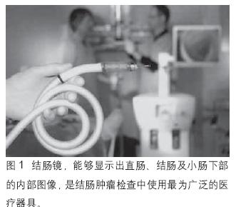
Analysis on the development prospect of medical technology with low-cost CMOS image sensor
Analysis on the development prospect of medical technology with low-cost CMOS image sensor