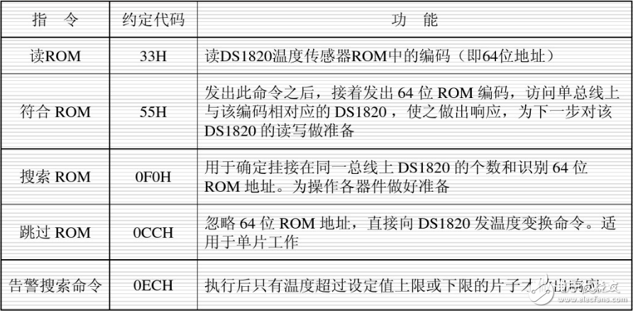
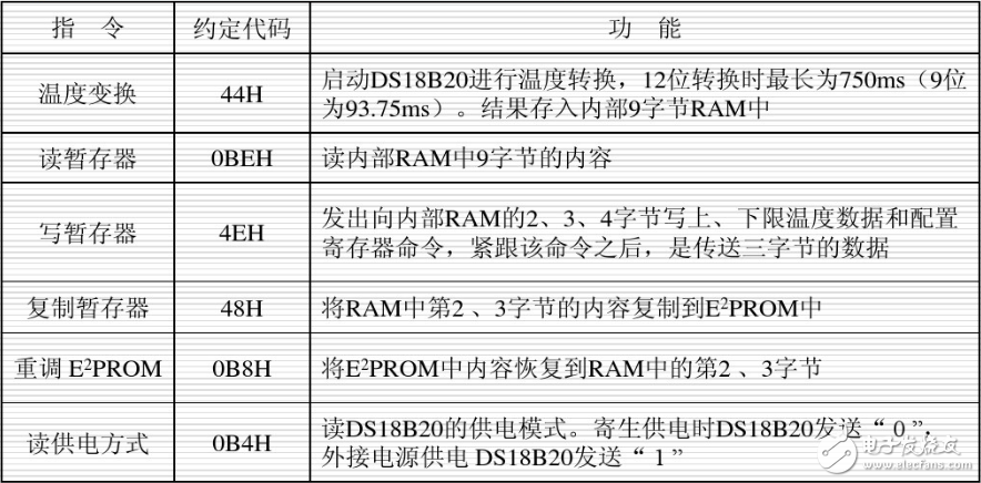
The single bus is the one-wire bus, which is the peripheral serial expansion bus technology introduced by DALLAS. Different from SPI and I2C serial data communication. It uses a single signal line to transmit both clock and data, and the data transmission is bidirectional. It has the advantages of saving I/O lines, simple resource structure, low cost, convenient bus expansion and maintenance. The single bus is a protocol developed by DALLAS. The system consists of a bus master node or multiple slave nodes. The data is read from the chip through the root signal line pair. Each slave chip that complies with the OneWire protocol has a unique address, including a 48-bit serial number, an 8-bit family code, and an 8-bit CRC code. The addressing of the master chip to each slave chip is based on the difference of 64 bits. A single bus utilizes one wire for two-way communication. Therefore, the protocol has stricter requirements on timing, such as timings such as response, which have clear time requirements. The basic timing includes reset and acknowledge timing, write one bit timing, and read one bit timing. In the reset and acknowledge timing, after the master sends a reset signal, the slave is required to send back the acknowledge signal within the specified time; in the bit read and bit write timing, the master reads or writes the data within the specified time. . The single bus is suitable for single-master systems and can control one or more slave devices. The host can be a microcontroller, and the slave can be a single bus device, and the data exchange between them passes through only one signal line. When there is only one slave device, the system can operate as a single node system; when there are multiple slave devices, the system operates as a multi-node system. A single bus device is internally provided with a parasite power circuit (Parasite Power Circuit). When the single bus is at a high level, the chip is powered by the diode VD on the one hand, and the internal capacitor C (about 800 pF) is charged on the other hand; when the single bus is at a low level, the diode is turned off, and the internal capacitor c supplies power to the chip. Since the capacity of the capacitor c is limited, it is required that the single bus can be supplied with a high level at intervals to continuously charge the internal capacitor C and maintain the normal operation of the device. This is how the "parasitic power" of "stealing" power through a network line works. It should be noted that in order to ensure that some devices on the bus have sufficient current supply during operation (such as temperature sensor temperature conversion, E2PROM writes human data), in addition to the pull-up resistor, the MOSFET needs to be used on the bus. (Field effect transistor) provides strong pull-up power. The data transmission rate of a single bus is generally 16.3 Kbit/s, and the maximum is 142 Kbit/s. Normally, data is transmitted at a rate of 100 Kbit/s or less. The main equipment I/O port can directly drive slave devices in the range of 200m, and can be extended to 1km. In order to explain the process of single bus data transmission, the following describes the single bus data communication transmission process in four parts, which are single bus communication signal type, single bus communication initialization, single bus communication ROM command and single bus communication. Function command. The single bus communication protocol defines the following types: reset pulse, acknowledge pulse, write 0, write 1, read 0, and read 1. Except for the acknowledge pulse, all signals are sent by the master to synchronize signals, and all transmitted Commands and data are both low-order first. Different types of signals in a single bus communication protocol use a waveform representation similar to pulse width modulation. Logic 0 is represented by a longer low level sustain period, and logic 1 is represented by a longer high level sustain period. In the single-bus communication protocol, the concept of reading and writing time slots is very important. When the system host outputs data to the slave device, a write time slot is generated. When the host reads data from the slave device, a read time slot is generated, and each time slot bus is generated. Only one bit of data can be transferred. Whether in the read time slot or the write time slot, they start with the host driving the data line bit low level, and the falling edge of the data line is the delay circuit of the internal trigger device to synchronize with the host. Within the write time slot, the delay circuit determines the time window in which the slave device samples the data line. There are two types of write slots in a single bus communication protocol: write 1 and write 0. The master writes 1 to the slave with a write 1 time slot and 0 to the slave with a write 0 time slot. All write time slots are at least 60 us, and at least 1 us recovery time is required between two separate write time slots. Both write time slots start with the host pulling the data bus low. The method of generating 1 time slot: after the host pulls the bus low, the bus must be released within 15us, and the bus is pulled to the high level by the pull-up resistor; the way of writing the 0 time slot is that after the host is pulled low, only Keep low for the entire time slot (at least 60us). The single bus device samples the total level state during the 15us~60us period after the start of the write time slot. If the sampled value is high during this time, a logic 1 is written to the device; if it is 0, a logic 0 is written. In the figure below, the black implementation represents the system host pulling the bus low, and the black dashed line represents the pull-up resistor pulling the bus high. For read time slots, a single bus device transmits data to the host only when the host issues a read time slot. After all hosts issue a read data command, a read time slot must be generated immediately so that the slave can transfer data. All read time slots require at least 60 us, and at least 1 us recovery time is required between two independent read time slots. Each read time slot is initiated by the host, at least pulling the bus 1us low. After the host issues a read time slot, the single bus device begins transmitting 0 or 1 on the bus. If the slave sends a 1, the bus is held high; if 0 is issued, the bus is pulled low. When 0 is transmitted, the slave releases the bus after the end of the read time slot, and the pull-up resistor pulls the bus back to the idle high state. The data sent by the slave remains valid for 15us after the start time slot, so the master must release the bus during the read time slot and sample the bus state within 15us after the start of the time slot. The black solid line in the above figure represents the system host pulling the bus low, the gray solid line represents the pull-down of the bus, and the black dotted line represents the pull-up resistor bus pull-up. The above describes several signals in the single bus communication process, but since the reset pulse is closely related to the initialization of the single bus communication process, the introduction of these two signals will be described in the single bus communication initialization. All communication on a single bus starts with an initialization sequence that includes a reset pulse from the master and an acknowledge pulse from the slave, as shown in the following figure. In the figure, the solid black line represents the system host pulling the bus low, the gray solid line represents the slave pulls the bus low, and the black dashed line represents the pull-up resistor that loves the bus pull-up. The reset pulse sent by the system master sends a low level of 480us~960us, and then releases the bus into the accept state. At this time, the system bus is connected to VCC high level through a 4.7K pull-up resistor for about 15us~60us. The device inoculated at the receiving end starts detecting the falling edge on the I/O pin and monitoring the arrival of the pulse. The master device is in this state for at least 480us. As a miracle of the slave device, after receiving the reset pulse from the system master device, it sends an acknowledge pulse to the bus, indicating that the slave device is ready to send or receive data according to various commands. Normally, the device waits for 15us~60us to send an acknowledge pulse (the pulse is a low level signal of 60us~240us, which is forced by the slave to pull the bus low). The reset pulse master is issued in a broadcast manner, so all slave devices on the bus simultaneously send acknowledge pulses. Once the device detects the acknowledge pulse, the master considers that the slave device is connected to the bus and the master device will then send the relevant ROM function command. If the master fails to detect the acknowledge pulse, then the single bus slave is not considered to be attached to the bus. When the host detects the acknowledge pulse, it issues a ROM command that is associated with the unique 64-bit ROM code of each slave device, allowing the master to specify the operation of a slave device when multiple slave devices are connected on a single bus. Enables the host to operate a slave device. These commands enable the host to detect how many slave devices and device types are on the bus, or whether the device is in an alarm state. The slave device supports five ROM commands, each of which is 8 bits long. Before the machine is issued, the machine must issue a ROM command. ROM command table The host issues a ROM command, accesses the specified slave, and then issues a function command. These commands allow the host to write or read the slave register, start the job, and determine how the slave is powered.
·Basic precautions
Do not put expensive oil into low-quality cartridges to avoid wastage. Most pre-filled oil cartridges have the so-called 510 thread. The oil cartridge screws onto a rechargeable battery. Some of these batteries have buttons and some heat up automatically when you pump the oil. Some batteries have multiple temperature settings and some heat up to a preset temperature; these features need to be known in advance.
·Cleaning notes
Use a suitable cleaning tool to clean them, such as activated charcoal or dried tea leaves in a used pipe to absorb the oil. It is important not to use alcohol or other boiling water to clean the pipe, and to wait until it has cooled down completely before cleaning. Otherwise, the hot stem will come into contact with the watery liquid and cause the mouthpiece tenon to loosen, thus shortening the life of the 510 cartridges.
This is what you should be aware of when using 510 cartridges. At the same time, when using 510 cartridges, there are still some vaping tips, for example, when using them, be careful not to suck too hard, will not produce smoke. When you inhale too hard, the smoke is sucked directly into your mouth and not atomized by the atomizer, so gently inhaling is more powerful and gives you a better vaping experience.
510 Cartridge Oem,Leakproof 510 Cartridge,510 Battery And Cartridges Oem,510 Cartridge Shenzhen MASON VAP Technology Co., Ltd. , https://www.disposablevapepenfactory.com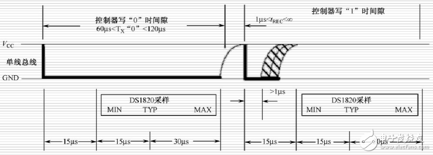
Single bus communication write time slot timing diagram 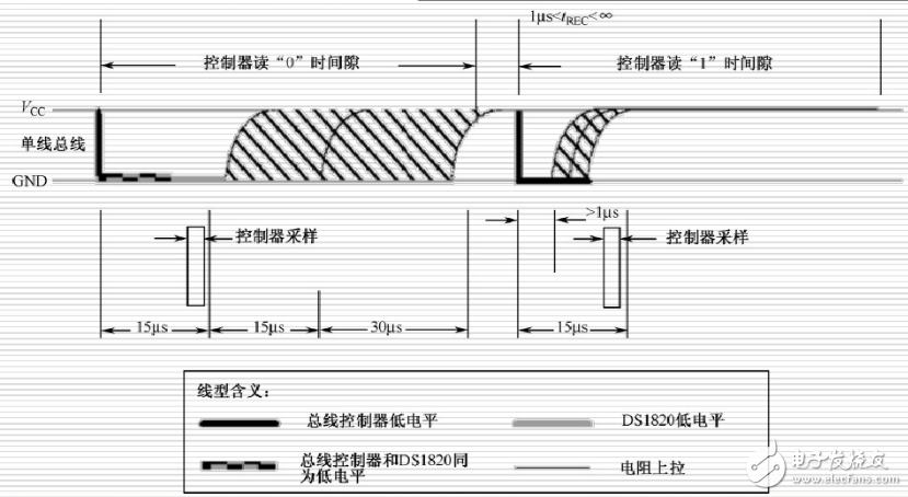
Single bus communication read time slot timing diagram 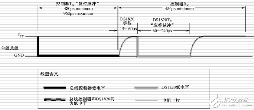
Bus communication initialization diagram 